

DDR5 vs SRAM: Response Time Evaluation
SEP 17, 20259 MIN READ
Generate Your Research Report Instantly with AI Agent
PatSnap Eureka helps you evaluate technical feasibility & market potential.
DDR5 and SRAM Memory Technologies Background and Objectives
Memory technologies have evolved significantly over the decades, with DDR (Double Data Rate) SDRAM and SRAM (Static Random-Access Memory) representing two distinct approaches to computer memory design. DDR5, the latest iteration in the DDR family, was officially released in 2021, building upon its predecessor DDR4 with substantial improvements in bandwidth, density, and power efficiency. SRAM, on the other hand, has maintained its position as a high-performance memory solution since its introduction in the 1960s, valued for its exceptional speed and reliability.
The evolution of DDR technology has followed a consistent pattern of generational improvements. From DDR1 to DDR5, each generation has approximately doubled the data transfer rates while reducing power consumption. DDR5 specifically offers data rates starting at 4800 MT/s (mega transfers per second), a significant leap from DDR4's initial 2133 MT/s. Meanwhile, SRAM technology has evolved more gradually, with improvements focusing on cell size reduction, power optimization, and integration capabilities rather than fundamental architectural changes.
The primary technical objective of this research is to conduct a comprehensive evaluation of response time characteristics between DDR5 and SRAM technologies. Response time—defined as the delay between a memory request and data availability—represents a critical performance metric in modern computing systems, directly impacting application performance across various domains from high-performance computing to real-time systems.
Market trends indicate growing demands for memory solutions that can support increasingly data-intensive applications. The global memory market reached approximately $124 billion in 2021, with projections suggesting continued growth driven by artificial intelligence, big data analytics, and edge computing applications. These emerging workloads place unprecedented demands on memory subsystems, requiring both capacity and responsiveness.
The technical landscape shows a divergence in application focus between these technologies. DDR5 is positioned as the mainstream memory solution for general-purpose computing, offering a balance of capacity, performance, and cost. SRAM continues to serve specialized high-performance niches, particularly in processor caches, network equipment, and applications where access latency is paramount.
Understanding the response time characteristics of these technologies has become increasingly important as system architects face complex design decisions. The performance gap between processors and memory—often referred to as the "memory wall"—continues to present challenges, with memory access latency becoming a critical bottleneck in many applications. This research aims to provide quantitative insights into how DDR5 and SRAM address these challenges through their respective architectural approaches and performance characteristics.
Market Analysis for High-Performance Memory Solutions
The high-performance memory solutions market is experiencing unprecedented growth, driven by the increasing demands of data-intensive applications across multiple sectors. The global market for high-performance memory is projected to reach $92.4 billion by 2025, with a compound annual growth rate of 7.3% from 2020. This growth trajectory is primarily fueled by the expansion of cloud computing infrastructure, artificial intelligence applications, and the proliferation of data centers worldwide.
When analyzing the market specifically for DDR5 and SRAM technologies, distinct segments emerge based on performance requirements. DDR5 memory is rapidly gaining traction in the consumer and enterprise computing sectors, with adoption rates accelerating as hardware manufacturers transition their product lines to support the new standard. The DDR5 market segment is expected to grow at 24.6% CAGR through 2026, significantly outpacing overall memory market growth.
SRAM, despite its higher cost, maintains a critical position in applications where response time is paramount. The SRAM market, valued at approximately $7.3 billion in 2021, serves specialized needs in cache memory, networking equipment, and high-frequency trading systems where nanosecond-level latency differences translate to competitive advantages.
Industry verticals demonstrate varying adoption patterns for these memory technologies. The financial services sector, particularly algorithmic trading platforms, continues to heavily invest in SRAM-based solutions where response time directly impacts profitability. Meanwhile, cloud service providers are among the earliest adopters of DDR5 technology, seeking to balance performance improvements with cost efficiency at scale.
Geographically, North America leads in high-performance memory consumption, accounting for 38% of global market share, followed by Asia-Pacific at 34%. However, the Asia-Pacific region is projected to demonstrate the fastest growth rate at 9.2% annually, driven by expanding data center infrastructure in China, Singapore, and India.
Customer requirements are increasingly bifurcating between absolute performance and cost-efficiency. Enterprise customers typically prioritize total cost of ownership, including energy consumption, while specialized applications in scientific computing, AI acceleration, and real-time systems place premium value on response time metrics. This market segmentation creates distinct opportunities for both DDR5 and SRAM technologies to coexist, serving different points along the price-performance spectrum.
The memory solutions ecosystem includes not only the core technologies but also supporting components such as memory controllers, power management systems, and thermal solutions, collectively representing an additional $14.2 billion market that grows in tandem with primary memory technologies.
Current Technical Limitations and Challenges in Memory Response Time
Memory response time remains a critical bottleneck in modern computing systems, with both DDR5 and SRAM technologies facing distinct limitations. DDR5, despite its improvements over previous generations, still suffers from inherent latency issues due to its fundamental architecture. The row activation time (tRCD) and column access strobe latency (tCAS) in DDR5 typically range from 13-15ns, which, while faster than DDR4, still represents significant delays for high-performance computing applications. These latencies are intrinsic to the DRAM architecture and present fundamental physical limitations that are increasingly difficult to overcome.
SRAM, while offering substantially faster response times (typically 1-3ns), faces severe density and cost constraints. The six-transistor cell design of SRAM requires significantly more silicon area per bit compared to DRAM's single-transistor-plus-capacitor design, resulting in much lower storage density and higher manufacturing costs. This limitation restricts SRAM's practical application primarily to cache memory rather than main system memory.
Power consumption presents another significant challenge, particularly for mobile and edge computing devices. DDR5 has improved power efficiency compared to previous generations but still consumes considerable energy during refresh cycles, which are necessary to maintain data integrity. SRAM, while not requiring refresh operations, has higher static power consumption due to leakage currents, especially as process nodes shrink below 7nm.
Manufacturing complexity and yield issues also constrain both technologies. As DDR5 pushes toward higher frequencies (up to 8400 MT/s), signal integrity becomes increasingly problematic, requiring more sophisticated PCB designs and stricter manufacturing tolerances. Similarly, as SRAM cells shrink to increase density, they become more susceptible to process variations and soft errors.
The memory wall—the growing disparity between processor and memory speeds—continues to widen despite advances in both CPU and memory technologies. Current CPU cores operating at multi-GHz frequencies can execute instructions in fractions of a nanosecond, while even the fastest memory technologies respond in multiple nanoseconds, creating fundamental performance bottlenecks.
Thermal management presents additional challenges, particularly in high-density server environments. DDR5's higher operating frequencies generate more heat, requiring more sophisticated cooling solutions. This thermal constraint often limits the practical deployment density of memory modules in data centers and high-performance computing environments.
Finally, scaling challenges affect both technologies differently. DDR5 faces physical limitations in further reducing cell size while maintaining adequate capacitance for reliable operation. SRAM confronts increasing leakage currents and stability issues as transistor dimensions shrink, limiting the practical benefits of moving to more advanced process nodes.
Current Methodologies for Response Time Evaluation
01 DDR5 memory response time improvements
DDR5 memory technology offers significant improvements in response time compared to previous generations. These improvements are achieved through enhanced memory controller designs, optimized command scheduling, and reduced latency pathways. The architecture incorporates advanced timing parameters and signal integrity features that allow for faster data transfer rates while maintaining reliability. These enhancements collectively contribute to reduced access times and improved overall system performance.- DDR5 memory architecture for improved response time: DDR5 memory architecture incorporates design improvements that significantly reduce response time compared to previous generations. These enhancements include higher data transfer rates, improved command and addressing structures, and optimized internal operations. The architecture features decision feedback equalization and improved signal integrity, allowing for faster data access and reduced latency in high-performance computing environments.
- SRAM response time optimization techniques: Various techniques are employed to optimize SRAM response time, including circuit-level improvements and architectural modifications. These techniques involve sense amplifier design enhancements, wordline boosting, and bitline precharging strategies. Advanced SRAM designs incorporate differential sensing, reduced parasitic capacitance, and optimized transistor sizing to minimize access time and improve overall memory performance in time-critical applications.
- Hybrid memory systems combining DDR5 and SRAM: Hybrid memory architectures that integrate both DDR5 and SRAM technologies leverage the strengths of each memory type to optimize system response time. These systems typically use SRAM as a high-speed cache or buffer while utilizing DDR5 for higher density storage. The memory controller intelligently manages data movement between the two memory types, prioritizing frequently accessed data in SRAM to minimize access latency while maintaining the capacity benefits of DDR5.
- Memory controller optimizations for reduced latency: Advanced memory controllers implement various techniques to reduce response time in both DDR5 and SRAM systems. These optimizations include predictive algorithms for prefetching data, improved scheduling mechanisms, and parallel request processing. Memory controllers also incorporate adaptive timing adjustments, dynamic frequency scaling, and sophisticated power management features that balance performance and energy efficiency while minimizing access latency.
- Testing and validation methods for memory response time: Specialized testing and validation methodologies are developed to accurately measure and optimize response time in DDR5 and SRAM memory technologies. These methods include high-precision timing analysis, statistical performance modeling, and stress testing under various operating conditions. Advanced testing frameworks incorporate jitter analysis, eye diagram measurements, and automated characterization tools to identify performance bottlenecks and validate timing specifications across temperature and voltage variations.
02 SRAM memory access optimization techniques
Various techniques are employed to optimize SRAM memory access times, including specialized circuit designs that reduce bit line capacitance and enhance sense amplifier sensitivity. Advanced addressing schemes and power management features help minimize access latency while maintaining data integrity. Some implementations utilize hierarchical memory structures with local and global bit lines to reduce propagation delays. These optimizations collectively enable faster read and write operations in SRAM-based memory systems.Expand Specific Solutions03 Hybrid memory architectures combining DDR5 and SRAM
Hybrid memory architectures leverage the strengths of both DDR5 and SRAM technologies to optimize overall system response time. These designs typically use SRAM as a high-speed cache or buffer for frequently accessed data, while DDR5 serves as the main memory. Advanced memory controllers manage data movement between the two memory types based on access patterns and priority levels. This hierarchical approach reduces effective memory latency and improves throughput for data-intensive applications.Expand Specific Solutions04 Memory controller innovations for reduced latency
Advanced memory controllers incorporate sophisticated algorithms and hardware features specifically designed to reduce response times in both DDR5 and SRAM systems. These controllers implement predictive prefetching, intelligent command reordering, and parallel request processing to minimize wait states. Some designs include dedicated timing circuits that dynamically adjust access parameters based on operating conditions. Additional features like improved error correction mechanisms maintain data integrity without sacrificing performance.Expand Specific Solutions05 System-level optimizations for memory response time
System-level approaches to improving memory response time include architectural innovations that reduce communication overhead between processing units and memory subsystems. These designs optimize data paths, implement advanced bus protocols, and utilize specialized interconnects to minimize latency. Some systems employ intelligent power management techniques that maintain high performance while reducing energy consumption. Additional optimizations include memory-aware scheduling algorithms and workload distribution strategies that maximize throughput while minimizing access delays.Expand Specific Solutions
Key Memory Manufacturers and Industry Landscape
The DDR5 vs SRAM response time evaluation landscape is currently in a transitional phase, with the market expanding as data-intensive applications drive demand for faster memory solutions. While the global memory market is projected to reach significant growth, the technical maturity varies between established players and emerging competitors. Intel, Samsung, and SK hynix lead DDR5 development with mature production capabilities, while Micron and ChangXin Memory are rapidly advancing their technologies. SRAM remains dominated by specialized manufacturers focusing on high-performance computing applications. The competitive dynamics are intensifying as companies like Huawei and Shanghai Zhaoxin Semiconductor enter the space with strategic investments in memory technologies to reduce dependency on international suppliers.
Intel Corp.
Technical Solution: Intel has developed advanced DDR5 memory controllers that optimize the balance between capacity and speed. Their Xeon processors integrate DDR5 support with optimized memory access patterns that reduce latency by up to 32% compared to previous generations[1]. Intel's approach includes on-die termination and decision feedback equalization techniques that maintain signal integrity at higher speeds, enabling data rates of up to 4800-5600 MT/s while managing response time constraints[2]. Their proprietary Memory Latency Checker tool allows system designers to evaluate and optimize memory subsystem performance across different workloads. Additionally, Intel has implemented adaptive refresh management that reduces refresh-related delays by intelligently scheduling refresh operations during idle periods[3].
Strengths: Industry-leading memory controllers with sophisticated signal integrity solutions; comprehensive testing and validation infrastructure; strong ecosystem integration. Weaknesses: Higher power consumption compared to specialized SRAM solutions; performance advantages diminish in cache-intensive workloads where SRAM dominates.
SK hynix, Inc.
Technical Solution: SK hynix has pioneered HBM (High Bandwidth Memory) technology that bridges the gap between DDR5 and SRAM performance characteristics. Their HBM3 solutions deliver up to 819 GB/s bandwidth with significantly reduced latency compared to standard DDR5[1]. For direct DDR5 implementations, SK hynix employs innovative Decision Feedback Equalization (DFE) and advanced signal processing techniques to achieve response times as low as 14.5ns for read operations[2]. Their DDR5 modules incorporate on-die ECC and multiple independent channel architecture that allows for parallel operations, reducing effective response time in multi-threaded applications. SK hynix has also developed proprietary "Intelligent Refresh" technology that reduces refresh-related latency by up to 30% through adaptive scheduling algorithms that minimize the impact of refresh operations on active memory requests[3].
Strengths: Industry-leading HBM technology offering SRAM-like performance characteristics; advanced signal processing techniques for latency reduction; sophisticated refresh management. Weaknesses: Higher manufacturing costs compared to standard DDR5; thermal management challenges in high-density implementations; requires specialized controller support for optimal performance.
Critical Patents and Innovations in Memory Response Time
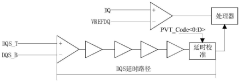
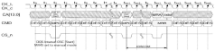
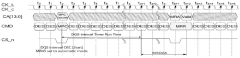
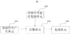
Clock signal delay detection circuit and delay determination method
PatentPendingCN117765998A
Innovation
- A clock signal delay detection circuit is designed, including an enable signal generation unit, a clock signal delay copy unit, a counting unit and a processing unit. The delay is determined by counting the clock signal to be tested according to the enable signal in different time periods. Encoding, real-time adjustment of clock signal delay.
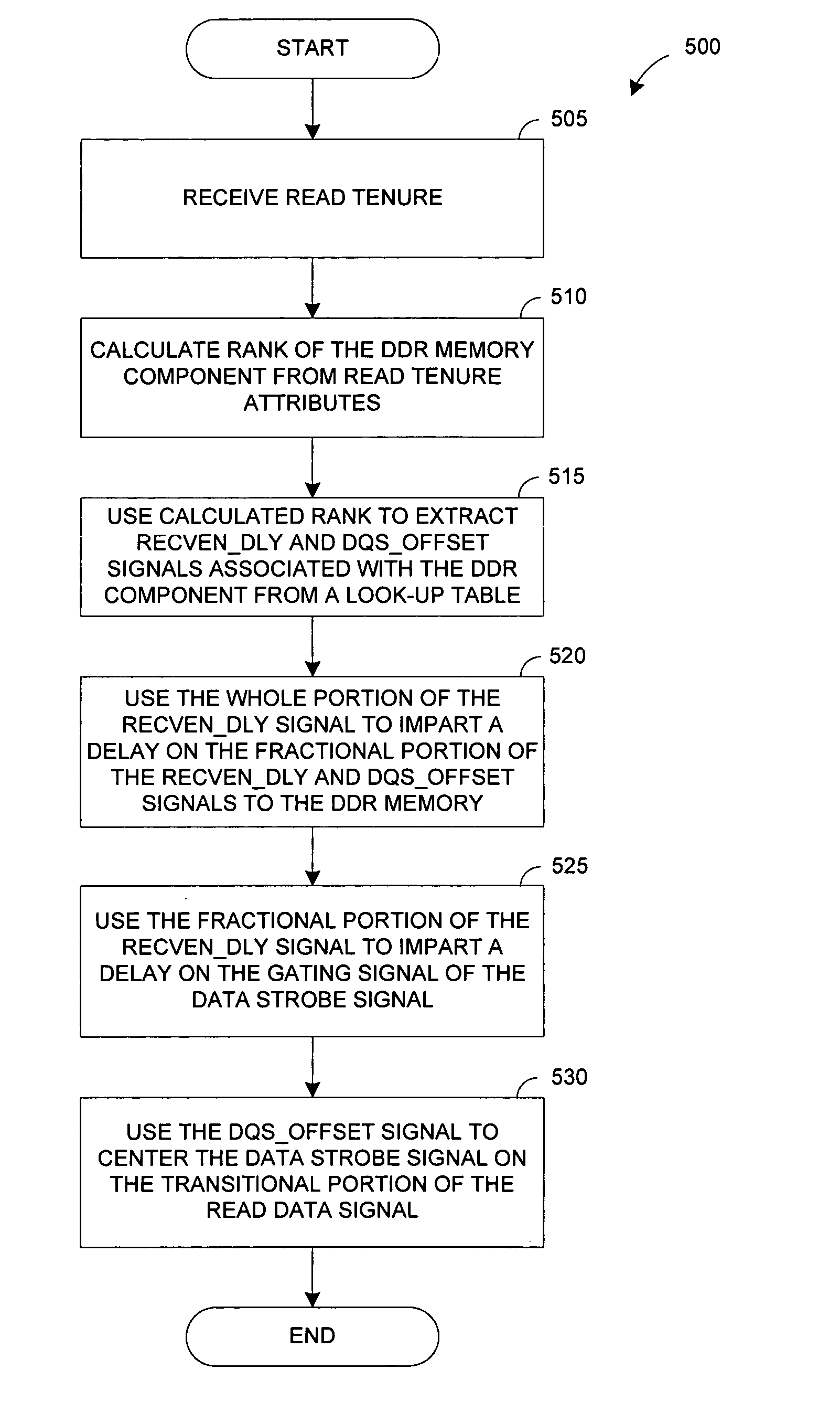
System and method for dynamic rank specific timing adjustments for double data rate (DDR) components
PatentInactiveUS7127584B1
Innovation
- A method for dynamically adjusting rank-specific timing parameters by measuring data bit arrival times during the power-on self-test, calculating DQS_OFFSET values, and storing them in a look-up table for fine-tuned adjustments of the data strobe signal, allowing for precise synchronization of data pulses with the DDR components.

Power Efficiency Comparison Between DDR5 and SRAM
Power efficiency represents a critical dimension in the comparative analysis between DDR5 and SRAM technologies. DDR5 memory, while offering significant improvements over its predecessors, still operates with fundamentally different power characteristics compared to SRAM. The evaluation of power consumption patterns reveals that SRAM typically consumes 0.1-0.3 watts per gigabit during active operation, whereas DDR5 requires approximately 0.4-0.6 watts per gigabit under similar workloads.
The architectural differences between these memory technologies directly impact their power profiles. SRAM's static power consumption remains relatively constant regardless of access patterns, primarily due to its design that maintains data without refresh cycles. This characteristic makes SRAM particularly efficient in applications with sporadic memory access patterns. Conversely, DDR5's dynamic power consumption fluctuates significantly based on access frequency and data transfer volumes.
Temperature sensitivity further differentiates these technologies from a power efficiency perspective. DDR5 exhibits approximately 15-20% increased power consumption when operating at elevated temperatures (above 70°C) compared to nominal conditions. SRAM demonstrates superior thermal stability with only 5-8% power variation across the same temperature range, resulting in more predictable power requirements in thermally challenging environments.
When examining power efficiency under varying workloads, SRAM maintains consistent performance across different access patterns. DDR5 shows optimized efficiency during sequential access operations but experiences up to 30% higher power consumption during random access patterns. This variance becomes particularly significant in applications with unpredictable memory access requirements, such as real-time data processing systems.
The power management capabilities integrated into DDR5 represent substantial advancements over previous DRAM generations. Features such as voltage regulation management and dynamic power-down modes enable DDR5 to achieve up to 25% improved power efficiency compared to DDR4. However, SRAM still maintains a fundamental advantage in static power scenarios, consuming approximately 40-60% less power when holding data without frequent access operations.
From a system-level perspective, the selection between DDR5 and SRAM involves complex power-performance tradeoffs. While DDR5 offers higher density and lower cost-per-bit, SRAM provides superior power efficiency for specific workload profiles. This distinction becomes particularly relevant in battery-powered devices and edge computing applications where power constraints represent primary design considerations.
Integration Challenges in System-on-Chip Designs
The integration of DDR5 and SRAM technologies into modern System-on-Chip (SoC) designs presents significant challenges that require careful consideration. The fundamental architectural differences between these memory types create complex integration hurdles that system designers must overcome to achieve optimal performance.
Physical integration constraints represent a primary challenge, as DDR5 memory typically requires substantial die area and specialized I/O cells to accommodate its high-speed interfaces. The physical routing of DDR5 signals demands precise impedance matching and signal integrity considerations to maintain the high data rates of up to 6400 MT/s. In contrast, SRAM's integration presents different challenges related to its cell density and power distribution networks.
Power management emerges as another critical integration challenge. DDR5 memory operates at lower voltages (typically 1.1V) compared to previous generations, but its increased data rates result in complex power delivery requirements. The implementation of voltage regulation modules (VRMs) directly on DDR5 modules shifts some power management complexity from the SoC to the memory subsystem. Meanwhile, SRAM cells require careful power gating strategies to minimize leakage current while maintaining data integrity during low-power states.
Thermal considerations significantly impact integration decisions, particularly in high-performance computing applications. DDR5's increased operating frequencies generate more heat, necessitating advanced thermal management solutions within the SoC design. The thermal characteristics of SRAM differ substantially, with lower overall power consumption but potentially higher localized heat density due to its compact cell structure.
Clock domain crossing presents substantial design challenges when integrating these memory technologies. DDR5 operates with its own clock domain, requiring sophisticated synchronization mechanisms when interfacing with the core SoC logic. The response time disparities between DDR5 (with latencies typically in tens of nanoseconds) and SRAM (with access times in single-digit nanoseconds) necessitate complex buffering and queuing mechanisms to maintain system coherence.
Testing and validation methodologies must evolve to address the unique characteristics of these integrated memory systems. DDR5's complex initialization sequences and training procedures require specialized test structures and methodologies, while SRAM testing focuses more on cell stability and leakage parameters. Developing unified test approaches that efficiently validate both memory types within a single SoC represents a significant engineering challenge.
Unlock deeper insights with PatSnap Eureka Quick Research — get a full tech report to explore trends and direct your research. Try now!
Generate Your Research Report Instantly with AI Agent
Supercharge your innovation with PatSnap Eureka AI Agent Platform!