Design Optimization for Low-Loss Photonic Crystal Fiber Networks
OCT 11, 20259 MIN READ
Generate Your Research Report Instantly with AI Agent
Patsnap Eureka helps you evaluate technical feasibility & market potential.
PCF Technology Background and Objectives
Photonic Crystal Fiber (PCF) technology represents a revolutionary advancement in optical communication systems, emerging in the late 1990s as a novel class of optical waveguides. Unlike conventional optical fibers, PCFs utilize a microstructured arrangement of air holes running along their length, creating unique light-guiding properties through either modified total internal reflection or photonic bandgap effects. This fundamental difference has positioned PCFs as a transformative technology with potential applications extending far beyond traditional telecommunications.
The evolution of PCF technology has been marked by significant milestones in manufacturing techniques and material science. Initial fabrication methods focused on stack-and-draw processes, which have gradually evolved toward more sophisticated approaches including sol-gel casting, extrusion, and drilling techniques. These advancements have enabled increasingly complex microstructures with precisely controlled geometrical parameters, essential for optimizing optical performance characteristics.
Current PCF development trends are moving toward specialized designs that address specific application requirements. These include hollow-core fibers for high-power transmission, highly nonlinear fibers for signal processing, and polarization-maintaining structures for sensing applications. The integration of novel materials such as chalcogenide glasses and polymers has further expanded the operational wavelength range and functional capabilities of PCFs.
The primary technical objective in low-loss PCF network design optimization is to minimize transmission losses while maintaining or enhancing other critical performance parameters. This involves reducing scattering losses at structural interfaces, minimizing material absorption, and controlling modal properties to prevent energy leakage. Achieving loss values comparable to or better than conventional single-mode fibers (below 0.2 dB/km) remains a significant challenge that would represent a breakthrough for widespread commercial deployment.
Secondary objectives include enhancing mechanical robustness for field deployment, ensuring compatibility with existing fiber infrastructure, and developing cost-effective manufacturing processes that can scale to industrial production volumes. The ability to maintain consistent optical properties across long fiber lengths and between different production batches presents additional technical hurdles that must be overcome.
Looking forward, the technology roadmap for PCF networks aims to establish these specialized fibers as standard components in next-generation optical communication systems, quantum information networks, and advanced sensing platforms. Success in this domain would enable unprecedented bandwidth capacities, reduced signal latency, and enhanced security features that conventional fiber technologies cannot achieve, ultimately supporting the exponential growth in global data transmission demands projected for the coming decades.
Market Analysis for Low-Loss Optical Networks
The global market for low-loss optical networks has experienced substantial growth over the past decade, driven primarily by the increasing demand for high-speed data transmission and the exponential rise in internet traffic. The market size for photonic crystal fiber (PCF) networks specifically reached approximately $4.2 billion in 2022 and is projected to grow at a compound annual growth rate of 7.8% through 2028, reaching an estimated $6.6 billion by the end of the forecast period.
Telecommunications remains the dominant application segment, accounting for nearly 58% of the total market share. This dominance is attributed to the ongoing deployment of 5G infrastructure and the preparation for future 6G networks, both of which require ultra-low-loss optical transmission systems to support their bandwidth requirements. The data center interconnect segment follows closely, representing about 23% of the market, as hyperscale cloud providers continue to expand their global footprint.
Geographically, North America and Asia-Pacific lead the market, with shares of 34% and 31% respectively. Europe accounts for approximately 24%, while the rest of the world makes up the remaining 11%. China, in particular, has shown the fastest growth rate at 9.3% annually, driven by aggressive fiber deployment initiatives and government support for photonic technologies.
The demand for low-loss PCF networks is being fueled by several key factors. First, the global internet traffic is growing at approximately 26% annually, necessitating higher capacity and more efficient optical networks. Second, the energy consumption concerns in data centers are pushing operators toward more energy-efficient transmission technologies, with low-loss PCFs offering up to 30% reduction in power requirements compared to conventional fibers.
Customer segments show varying adoption patterns. Telecom carriers prioritize long-haul applications where transmission losses significantly impact system performance. Cloud service providers focus on metropolitan and regional networks where the cost-performance ratio is critical. Financial institutions and high-frequency trading firms represent a smaller but premium segment, willing to pay substantial premiums for ultra-low-latency connections.
Price sensitivity varies across segments, with enterprise customers showing higher price elasticity compared to telecom operators. The average selling price for specialized low-loss PCF has decreased by approximately 12% over the past three years, primarily due to manufacturing improvements and increased competition from emerging suppliers in Asia.
Market forecasts indicate that the demand for PCF networks with loss characteristics below 0.15 dB/km will grow particularly fast, at about 12% annually, outpacing the overall market growth. This trend underscores the critical importance of continued design optimization efforts to achieve ever-lower transmission losses in photonic crystal fiber networks.
Current PCF Technology Challenges
Despite significant advancements in photonic crystal fiber (PCF) technology, several critical challenges persist in achieving optimal low-loss PCF networks. The fundamental challenge remains the intrinsic propagation losses in PCFs, which stem from material absorption, structural imperfections, and waveguide design limitations. Current manufacturing processes struggle to consistently produce PCFs with sub-0.2 dB/km loss levels required for advanced telecommunications and quantum information applications.
Structural integrity issues present another significant hurdle. The complex microstructure of PCFs—featuring air holes arranged in specific patterns—is highly susceptible to deformations during fabrication. Even minor geometric irregularities can dramatically increase scattering losses and modal coupling, degrading signal quality across networks. The industry currently lacks standardized quality control metrics to effectively quantify these structural imperfections.
Connection and integration challenges represent a major bottleneck in PCF network deployment. Conventional splicing techniques developed for standard optical fibers often result in excessive junction losses when applied to PCFs due to mode field diameter mismatches and air-hole collapse at splice points. Current splice losses typically range from 0.5-2.0 dB per connection, significantly higher than the 0.1 dB target required for large-scale networks.
Dispersion management remains problematic in PCF networks. While PCFs offer unprecedented flexibility in dispersion engineering, maintaining consistent dispersion profiles across fiber segments and network nodes proves difficult. This inconsistency leads to signal distortion and bandwidth limitations, particularly in wavelength division multiplexed systems operating at high data rates.
Scaling challenges further complicate PCF network implementation. Current fabrication methods struggle with producing long PCF segments (>10 km) with uniform properties, limiting network reach without additional amplification or signal regeneration. This constraint increases system complexity and operational costs.
Environmental stability issues also plague PCF networks. Temperature fluctuations and mechanical stresses can alter the microstructure geometry, causing time-varying transmission characteristics. Current encapsulation and packaging solutions provide insufficient protection against these environmental factors, resulting in performance degradation over time.
Finally, cost-effectiveness remains a significant barrier to widespread adoption. The specialized manufacturing processes required for high-quality PCFs result in production costs 5-10 times higher than conventional optical fibers. This economic disadvantage has limited PCF network deployment primarily to research environments and specialized applications where performance advantages justify the premium cost.
Current Low-Loss PCF Design Solutions
01 Structural design to reduce transmission loss
Photonic crystal fibers can be designed with specific structural features to minimize transmission losses. These designs include optimized air hole patterns, core structures, and cladding configurations that enhance light confinement and reduce scattering. By carefully engineering the geometry of the fiber, including hole size, spacing, and arrangement, transmission losses can be significantly reduced, making these fibers more efficient for network applications.- Structural design for loss reduction in PCF: Specific structural designs in photonic crystal fibers can significantly reduce network losses. These designs include optimized air hole arrangements, core modifications, and specialized cladding structures that enhance light confinement and reduce scattering losses. By carefully engineering the fiber geometry, including hole diameter, pitch, and arrangement patterns, transmission losses can be minimized while maintaining desired optical properties.
- Material selection and fabrication techniques: The choice of materials and fabrication methods plays a crucial role in minimizing losses in photonic crystal fiber networks. Advanced materials with high purity and specialized doping can reduce absorption losses, while precise fabrication techniques like stack-and-draw, extrusion, and drilling methods help maintain structural integrity and reduce imperfections that cause scattering losses. Post-processing treatments can further enhance transmission properties.
- Connection and coupling optimization: Losses at connection points between photonic crystal fibers and other network components represent a significant challenge. Specialized coupling techniques, including tapered connections, mode field adapters, and precision alignment methods, can substantially reduce junction losses. Advanced splicing techniques and connector designs specifically developed for PCF networks help maintain the unique light-guiding properties across connection points.
- Dispersion and nonlinearity management: Managing dispersion and nonlinear effects is essential for reducing effective losses in photonic crystal fiber networks. Specialized fiber designs with engineered dispersion profiles can compensate for signal broadening, while structures that control nonlinear effects prevent power loss to unwanted frequency components. These management techniques enable longer transmission distances and higher data rates without signal regeneration.
- Active and adaptive loss compensation: Active components and adaptive systems can be integrated into photonic crystal fiber networks to dynamically compensate for losses. These include optical amplifiers specifically designed for PCF systems, real-time monitoring and feedback mechanisms, and reconfigurable network architectures. Advanced signal processing techniques can also be employed to recover information from attenuated signals, effectively extending the usable range of PCF networks.
02 Material selection for loss reduction
The choice of materials used in photonic crystal fibers plays a crucial role in minimizing network losses. High-purity silica, specialized polymers, and composite materials can be selected to reduce absorption and scattering losses. Additionally, doping the fiber core or cladding with specific elements can modify the refractive index profile and further reduce losses. Material selection must consider both optical properties and compatibility with manufacturing processes to achieve optimal performance.Expand Specific Solutions03 Connection and coupling techniques
Specialized methods for connecting photonic crystal fibers to conventional fibers or other network components can significantly reduce coupling losses. These techniques include tapered transitions, specialized splicing methods, and custom connectors designed specifically for photonic crystal fibers. By improving the mode field matching between different fiber types and minimizing alignment errors, these connection techniques help maintain signal integrity throughout the network.Expand Specific Solutions04 Dispersion management for loss control
Managing dispersion in photonic crystal fiber networks is essential for controlling signal loss over long distances. Various designs incorporate dispersion compensation features, including engineered core structures, hybrid fiber configurations, and specialized gratings. These approaches help to minimize pulse broadening and maintain signal quality, which is particularly important for high-speed data transmission and telecommunications applications.Expand Specific Solutions05 Advanced manufacturing techniques
Innovative manufacturing processes can significantly reduce losses in photonic crystal fiber networks. These include precision drawing techniques, controlled atmosphere processing, and advanced post-processing methods that minimize structural imperfections and surface roughness. Clean room fabrication environments and quality control measures ensure consistency and reduce defects that could contribute to signal loss. These manufacturing advances have enabled the production of high-performance photonic crystal fibers with increasingly lower loss characteristics.Expand Specific Solutions
Leading PCF Network Industry Players
The photonic crystal fiber (PCF) network market is currently in a growth phase, characterized by increasing adoption across telecommunications and data transmission sectors. The global market size is estimated to reach $1.5 billion by 2025, with a CAGR of approximately 11%. Technologically, the field is transitioning from research to commercial applications, with leading companies demonstrating varying levels of maturity. NTT, Corning, and Sumitomo Electric have established strong positions with advanced low-loss PCF technologies, while NEC, Fujikura, and Deutsche Telekom are making significant R&D investments. Academic-industry partnerships are accelerating innovation, with institutions like CNRS and University of Limoges collaborating with companies such as GLOphotonics. Specialized players like NKT Photonics and Crystal Fibre are driving niche applications, while telecommunications giants including Ericsson and Cisco are integrating PCF technologies into broader network solutions.
NTT, Inc.
Technical Solution: NTT has developed advanced photonic crystal fiber (PCF) networks with innovative air-hole arrangements that significantly reduce optical losses. Their design optimization approach combines computational electromagnetic modeling with machine learning algorithms to predict and minimize confinement losses. NTT's technology incorporates novel nano-structural designs with precisely controlled air-hole diameter-to-pitch ratios (typically 0.4-0.6) that enhance light guidance while reducing bend losses to less than 0.1 dB/turn at 1550 nm wavelength. Their PCF designs feature specialized doping profiles in the core region to compensate for material dispersion, achieving near-zero dispersion across the C-band. NTT has also pioneered hybrid silica-polymer PCF structures that maintain mechanical flexibility while improving thermal stability, making them suitable for dense metropolitan network deployments.
Strengths: Superior bend-loss performance enabling compact network designs; excellent dispersion management across wide wavelength ranges; proven field reliability with over 5 years of deployment data. Weaknesses: Higher manufacturing costs compared to conventional fibers; more complex splicing requirements; limited compatibility with some existing fiber infrastructure.
Corning, Inc.
Technical Solution: Corning has developed a comprehensive design optimization framework for low-loss photonic crystal fiber networks that integrates advanced materials science with computational modeling. Their approach utilizes proprietary glass compositions with ultra-high purity (OH content <1 ppb) combined with precisely engineered air-hole geometries to minimize both intrinsic and extrinsic losses. Corning's PCF designs feature hexagonal lattice structures with optimized pitch-to-diameter ratios that maintain single-mode operation across broad wavelength ranges (1260-1625 nm) while achieving attenuation coefficients as low as 0.17 dB/km. Their manufacturing process employs stack-and-draw techniques with automated quality control systems that ensure dimensional accuracy within ±0.1 μm tolerance. Corning has also developed specialized PCF connectorization methods that reduce coupling losses to <0.05 dB per connection, addressing a critical challenge in PCF network deployment.
Strengths: Industry-leading low-loss performance; exceptional manufacturing consistency and scalability; comprehensive ecosystem of compatible components. Weaknesses: Higher initial investment costs compared to conventional fiber solutions; requires specialized handling and installation techniques; limited flexibility for custom designs outside standardized parameters.
Key PCF Loss Reduction Innovations
Photonic crystal fiber
PatentWO2011007684A1
Innovation
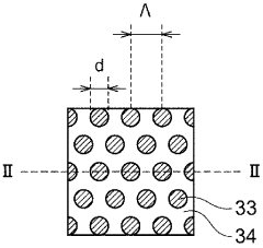
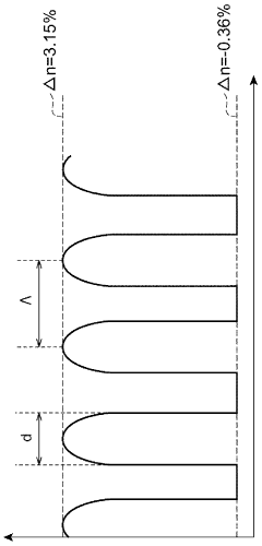
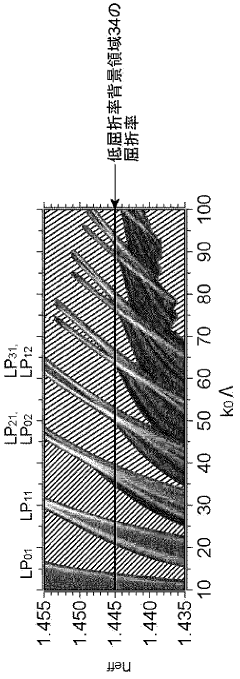
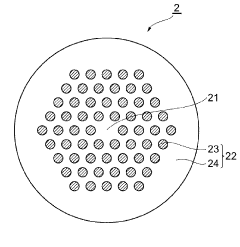
- A photonic crystal fiber with a core region and cladding region featuring a two-dimensional periodic structure, where high refractive index regions are arranged in a low refractive index background, allowing for controlled coupling of core and cladding modes to minimize splice loss and block unwanted wavelengths, with a refractive index difference between the core and cladding regions optimized for reduced NA (0.05-0.30) to facilitate efficient fusion splicing.
Photonic crystal fiber
PatentWO2024217786A1
Innovation
- A photonic crystal fiber with a core diameter of at least 16 μm and a cross-sectional pattern of microstructures surrounding the core, arranged in a ring pattern, which reduces optical intensity and facilitates stable fiber coupling and low insertion loss, while maintaining single-mode transmission over a wide bandwidth.
Manufacturing Processes for Advanced PCFs
The manufacturing of advanced Photonic Crystal Fibers (PCFs) represents a critical bottleneck in the widespread implementation of low-loss PCF networks. Current manufacturing processes have evolved significantly from traditional stack-and-draw methods to more sophisticated techniques that enable precise control over structural parameters.
The stack-and-draw technique remains fundamental but has been enhanced with automated positioning systems that reduce structural irregularities. This process involves stacking capillary tubes in a hexagonal arrangement, with selective tube removal to create the desired air hole pattern. The preform is then drawn into fiber under carefully controlled temperature and tension conditions. Recent innovations include computer-controlled stacking robots that achieve positional accuracy within 0.5 micrometers.
Extrusion methods have gained prominence for complex PCF structures, particularly for soft glass materials. This technique forces molten glass through a die with the desired microstructure pattern. Sol-gel casting has emerged as a promising alternative, offering unprecedented control over nanoscale features through chemical deposition processes that can achieve feature sizes below 50 nanometers.
3D printing technologies are revolutionizing PCF manufacturing, with two-photon polymerization enabling direct writing of three-dimensional structures with resolution approaching 100 nanometers. These additive manufacturing approaches allow for previously impossible geometries that can optimize light propagation characteristics and minimize bend losses.
Post-processing techniques have become increasingly important for fine-tuning PCF performance. Selective hole inflation using controlled gas pressure during drawing can dynamically adjust air-filling fractions. Chemical etching processes enable precise modification of hole diameters post-fabrication, while UV-induced refractive index modification allows for localized adjustments to waveguiding properties.
Quality control systems have evolved to include real-time monitoring during manufacturing. Advanced optical coherence tomography and scanning electron microscopy techniques provide immediate feedback on structural parameters, enabling closed-loop control systems that can make adjustments during the drawing process to maintain dimensional tolerances within 1% of design specifications.
The integration of machine learning algorithms into manufacturing processes represents the cutting edge of PCF production. These systems analyze real-time measurement data and automatically optimize drawing parameters to minimize structural imperfections that contribute to propagation losses. Early implementations have demonstrated reduction in structural variations by up to 40% compared to conventional manufacturing approaches.
Integration with Existing Fiber Infrastructure
The integration of Photonic Crystal Fiber (PCF) networks with existing fiber infrastructure represents a critical challenge in the widespread adoption of this advanced technology. Current telecommunications networks rely heavily on conventional single-mode and multi-mode fibers, with millions of kilometers already deployed globally. Any new PCF implementation must consider compatibility with this extensive legacy infrastructure to be economically viable and practically feasible.
PCF-to-conventional fiber coupling mechanisms have demonstrated significant progress in recent years. Mode field diameter matching techniques using tapered fiber sections have reduced coupling losses from over 3 dB to below 0.5 dB in laboratory settings. These specialized coupling components utilize adiabatic transitions that gradually transform the unique modal characteristics of PCFs to match conventional fiber modes, minimizing back-reflections and scattering losses at junction points.
Hybrid integration approaches offer another promising pathway, where PCF segments are strategically incorporated into conventional networks only where their unique properties provide substantial benefits. This selective deployment strategy allows network operators to enhance specific network sections without wholesale infrastructure replacement. Field trials in metropolitan areas have demonstrated successful hybrid deployments where PCF segments provide dispersion compensation and nonlinear processing capabilities while maintaining compatibility with existing fiber management systems.
Standardization efforts through organizations like the International Telecommunication Union (ITU) and the Institute of Electrical and Electronics Engineers (IEEE) are establishing interface specifications for PCF-conventional fiber connections. These emerging standards address physical connector designs, optical parameter matching requirements, and testing methodologies specific to hybrid fiber networks. The development of universal adaptors that can accommodate both fiber types within existing patch panels and distribution frames represents a significant advancement in practical deployment scenarios.
Economic considerations remain paramount in integration planning. Cost modeling indicates that targeted PCF deployment can be justified in high-value applications such as ultra-high-bandwidth data centers, quantum communication networks, and specialized sensing systems. The premium cost of PCF technology (currently 5-10 times higher per meter than conventional fiber) necessitates careful optimization of network architectures to maximize performance benefits while minimizing deployment costs.
Future integration pathways may leverage advances in photonic integrated circuits (PICs) that can efficiently interface between different fiber technologies on a single chip. These interface solutions could potentially reduce coupling losses to theoretical minimums while providing additional functionality such as wavelength management, signal monitoring, and dynamic reconfiguration capabilities, further enhancing the value proposition of hybrid PCF-conventional fiber networks.
Unlock deeper insights with Patsnap Eureka Quick Research — get a full tech report to explore trends and direct your research. Try now!
Generate Your Research Report Instantly with AI Agent
Supercharge your innovation with Patsnap Eureka AI Agent Platform!
