

Exploring Polypropylene Thin Films in Optoelectronic Devices
JUL 21, 20259 MIN READ
Generate Your Research Report Instantly with AI Agent
Patsnap Eureka helps you evaluate technical feasibility & market potential.
PP Film Tech Background
Polypropylene (PP) thin films have emerged as a promising material in the field of optoelectronic devices, marking a significant advancement in materials science and engineering. The exploration of PP films in this context represents a convergence of polymer science and optoelectronics, two rapidly evolving fields that have seen substantial growth over the past few decades.
The journey of PP films in optoelectronics began in the late 20th century when researchers started investigating the potential of polymeric materials in electronic applications. Initially, the focus was primarily on their insulating properties and mechanical flexibility. However, as the understanding of polymer physics and chemistry deepened, scientists began to recognize the unique optical and electronic properties that could be harnessed from carefully engineered PP films.
The development of PP films for optoelectronic applications has been driven by several key factors. Firstly, the increasing demand for flexible, lightweight, and cost-effective electronic components has pushed researchers to explore alternatives to traditional inorganic materials. Secondly, advancements in polymer processing techniques have enabled the production of ultra-thin, highly uniform PP films with tailored properties.
One of the critical milestones in this field was the discovery that PP films could be modified to exhibit enhanced optical transparency and controlled refractive indices. This breakthrough opened up new possibilities for their use in various optoelectronic devices, including organic light-emitting diodes (OLEDs), photovoltaic cells, and optical sensors.
The evolution of PP films in optoelectronics has also been closely tied to the development of surface modification techniques. Researchers have explored various methods to functionalize the surface of PP films, including plasma treatment, chemical grafting, and nanoparticle incorporation. These modifications have allowed for improved adhesion, charge transport, and light management properties, essential for high-performance optoelectronic devices.
In recent years, the focus has shifted towards developing PP films with advanced functionalities. This includes the creation of nanostructured PP films that can manipulate light at the nanoscale, leading to enhanced light absorption or emission in optoelectronic devices. Additionally, efforts have been made to integrate PP films with other materials, such as conductive polymers or metal oxides, to create hybrid structures with synergistic properties.
The current technological landscape sees PP films being investigated for a wide range of optoelectronic applications. These include flexible displays, wearable electronics, smart packaging, and next-generation solar cells. The versatility of PP films, combined with their low cost and ease of processing, positions them as a key material in the ongoing miniaturization and flexibilization of electronic devices.
Optoelectronic Market
The optoelectronic market has experienced significant growth in recent years, driven by advancements in technology and increasing demand for efficient and high-performance electronic devices. This market encompasses a wide range of applications, including displays, lighting, photovoltaics, and optical communication systems. The integration of polypropylene thin films in optoelectronic devices represents a promising area of development within this expanding market.
The global optoelectronic market is projected to continue its upward trajectory, with a compound annual growth rate (CAGR) expected to remain strong in the coming years. This growth is fueled by the rising adoption of optoelectronic components in various industries, such as consumer electronics, automotive, healthcare, and telecommunications. The increasing demand for energy-efficient lighting solutions, high-resolution displays, and advanced sensing technologies has been a key driver of market expansion.
In the context of polypropylene thin films for optoelectronic devices, there is a growing interest in their potential applications. These films offer several advantages, including low cost, flexibility, and ease of processing, which make them attractive for use in flexible electronics and displays. The market for flexible optoelectronic devices, in particular, is expected to see substantial growth as consumers and industries seek more versatile and durable electronic products.
The Asia-Pacific region dominates the optoelectronic market, with countries like China, Japan, and South Korea leading in both production and consumption. This regional dominance is attributed to the presence of major electronics manufacturers, government support for technological innovation, and a large consumer base. However, North America and Europe also play significant roles in the market, particularly in research and development of advanced optoelectronic technologies.
The integration of polypropylene thin films in optoelectronic devices aligns with the broader trend towards sustainable and eco-friendly materials in electronics manufacturing. As environmental concerns become increasingly important to consumers and regulators, the use of recyclable and biodegradable materials like polypropylene could become a competitive advantage in the market.
Despite the positive outlook, the optoelectronic market faces challenges such as supply chain disruptions, geopolitical tensions affecting trade, and the need for continuous innovation to meet evolving consumer demands. The successful integration of polypropylene thin films in optoelectronic devices will depend on overcoming technical hurdles and demonstrating clear advantages over existing materials in terms of performance, cost-effectiveness, and environmental impact.
In conclusion, the optoelectronic market presents significant opportunities for the development and application of polypropylene thin films in various devices. As the market continues to grow and evolve, innovations in materials and manufacturing processes will play a crucial role in shaping the future of optoelectronic technologies and their widespread adoption across industries.
PP Film Challenges
The development and application of polypropylene (PP) thin films in optoelectronic devices face several significant challenges that require innovative solutions. One of the primary obstacles is achieving the necessary optical properties for these applications. PP films typically exhibit high haze and low transparency, which can significantly impair the performance of optoelectronic devices that rely on clear light transmission.
Another major challenge lies in the surface properties of PP films. The inherently low surface energy of polypropylene results in poor adhesion and wettability, making it difficult to apply functional coatings or integrate the films with other materials in device fabrication. This limitation can lead to delamination issues and reduced device longevity.
The thermal stability of PP films at elevated temperatures poses another hurdle for their use in optoelectronic applications. Many device manufacturing processes and operational conditions involve high temperatures, which can cause PP films to deform or degrade, compromising their structural integrity and optical properties.
Achieving consistent and uniform thickness across large areas is also a significant challenge in PP film production for optoelectronic devices. Variations in thickness can lead to inconsistent optical and electrical properties, affecting device performance and reliability.
The electrical insulating nature of PP films presents a challenge in applications where charge transport is crucial. Modifying the electrical properties of PP films without compromising their other beneficial characteristics requires sophisticated engineering approaches.
Environmental stability is another concern, as PP films can degrade when exposed to UV radiation and certain chemicals, potentially limiting their long-term performance in outdoor or harsh environments.
Recyclability and environmental impact present additional challenges. While PP is recyclable, the additives and modifications required for optoelectronic applications may complicate the recycling process and raise environmental concerns.
Scaling up production of high-quality PP films for optoelectronic devices while maintaining cost-effectiveness is a significant industrial challenge. The need for specialized equipment and precise control over manufacturing parameters can increase production costs.
Lastly, meeting the stringent regulatory requirements for materials used in optoelectronic devices, particularly in sectors like healthcare and aerospace, poses a regulatory challenge for PP film manufacturers and device makers.
Addressing these challenges requires interdisciplinary research efforts, combining expertise in polymer science, optics, electronics, and materials engineering to develop innovative solutions that can unlock the full potential of PP thin films in optoelectronic applications.
Current PP Solutions
01 Manufacturing processes for polypropylene thin films
Various manufacturing processes are employed to produce polypropylene thin films, including extrusion, casting, and blown film techniques. These methods allow for the production of films with specific properties and thicknesses suitable for different applications.- Manufacturing processes for polypropylene thin films: Various manufacturing processes are employed to produce polypropylene thin films, including extrusion, casting, and blown film techniques. These methods allow for the production of films with specific properties such as thickness, orientation, and surface characteristics. The choice of manufacturing process can significantly impact the final film properties and its suitability for different applications.
- Composition and additives for enhanced film properties: Polypropylene thin films can be modified with various additives and composition adjustments to enhance their properties. These may include stabilizers, plasticizers, nucleating agents, and other polymers. Such modifications can improve the film's mechanical strength, thermal stability, optical properties, and barrier characteristics, making them suitable for a wide range of applications.
- Surface treatment and modification of polypropylene films: Surface treatments and modifications are applied to polypropylene thin films to enhance their properties such as adhesion, printability, and barrier characteristics. These treatments may include corona discharge, plasma treatment, chemical etching, or the application of functional coatings. Such modifications expand the range of applications for polypropylene films in packaging, labeling, and other industries.
- Multilayer and composite polypropylene film structures: Multilayer and composite polypropylene film structures are developed to combine the advantages of different materials. These structures may include layers of different types of polypropylene, other polymers, or functional materials. Such composite films can offer improved barrier properties, mechanical strength, and specific functionalities tailored for various applications in packaging, electronics, and other industries.
- Applications and end-use products of polypropylene thin films: Polypropylene thin films find applications in various industries due to their versatile properties. They are used in packaging materials, agricultural films, capacitor dielectrics, and as substrates for flexible electronics. The films can be further processed into products such as adhesive tapes, labels, and protective coverings. The specific properties of the films, such as transparency, strength, and barrier characteristics, determine their suitability for different end-use products.
02 Composition and additives for improved film properties
Polypropylene thin films can be enhanced by incorporating additives and modifying the polymer composition. These modifications can improve properties such as strength, clarity, barrier performance, and processability, making the films suitable for a wide range of applications.Expand Specific Solutions03 Surface treatment and modification of polypropylene films
Various surface treatment methods are used to modify the properties of polypropylene thin films. These treatments can enhance adhesion, printability, and other surface characteristics, making the films more suitable for specific applications such as packaging or lamination.Expand Specific Solutions04 Multi-layer polypropylene film structures
Multi-layer polypropylene film structures are developed to combine the benefits of different materials or to achieve specific performance characteristics. These structures can include barrier layers, tie layers, or layers with different polypropylene grades to optimize properties for various applications.Expand Specific Solutions05 Applications and specialized polypropylene films
Polypropylene thin films are used in various applications, including packaging, labels, capacitors, and textiles. Specialized films are developed for specific uses, such as heat-sealable films, oriented films, or films with enhanced optical properties, to meet the requirements of different industries.Expand Specific Solutions
Key Industry Players
The exploration of polypropylene thin films in optoelectronic devices is currently in an emerging phase, with the market showing promising growth potential. The global market for advanced materials in optoelectronics is expanding, driven by increasing demand for flexible and lightweight electronic components. Companies like Toray Industries, Sumitomo Chemical, and Asahi Kasei are at the forefront of developing innovative polypropylene-based materials for optoelectronic applications. The technology is progressing rapidly, with research institutions such as ETRI and Wake Forest University contributing to advancements. However, the field is still evolving, and further development is needed to fully realize the potential of polypropylene thin films in commercial optoelectronic devices.
Toray Industries, Inc.
Technical Solution: Toray Industries has developed advanced polypropylene thin films for optoelectronic devices, focusing on improving optical and electrical properties. Their approach involves creating biaxially oriented polypropylene (BOPP) films with enhanced transparency and surface smoothness[1]. The company has implemented a proprietary stretching technique that allows for precise control of film thickness and uniformity, crucial for optoelectronic applications[2]. Toray's films feature high light transmittance (>90%) in the visible spectrum and low haze (<1%), making them ideal for display technologies and photovoltaic devices[3]. Additionally, they have incorporated nanoscale additives to improve the film's dielectric properties, enhancing its performance in capacitive touch screens and flexible electronics[4].
Strengths: Superior optical clarity, excellent uniformity, and enhanced dielectric properties. Weaknesses: Potentially higher production costs due to specialized manufacturing processes and limited high-temperature applications compared to some inorganic alternatives.
Samsung Display Co., Ltd.
Technical Solution: Samsung Display has integrated polypropylene thin films into their advanced OLED display technologies. Their approach focuses on using polypropylene as a protective and functional layer in flexible and foldable displays. The company has developed a proprietary lamination process that allows for the seamless integration of ultra-thin polypropylene films (< 10 μm) with OLED panels[5]. These films serve multiple purposes, including enhancing the mechanical flexibility of the display, providing a moisture barrier, and improving light outcoupling efficiency[6]. Samsung has also implemented surface treatment techniques to modify the polypropylene film's surface energy, enabling better adhesion to other layers in the display stack and reducing interfacial defects[7]. Their latest innovations include incorporating quantum dot-infused polypropylene films to enhance color gamut and brightness in QLED-OLED hybrid displays[8].
Strengths: Expertise in large-scale production and integration with existing display technologies, strong synergy with other Samsung technologies. Weaknesses: Potential limitations in extreme bending scenarios, dependency on other proprietary technologies in the display stack.
PP Film Innovations
Polypropylene film, metal layer-integrated polypropylene film, film capacitor and film roll
PatentActiveUS20230340245A1
Innovation
- A polypropylene film with specific surface roughness parameters, including Svk and Spk values, is developed to reduce contact area between surfaces, enhance cushioning properties, and maintain dielectric strength, while also improving conveying properties and processability during winding.
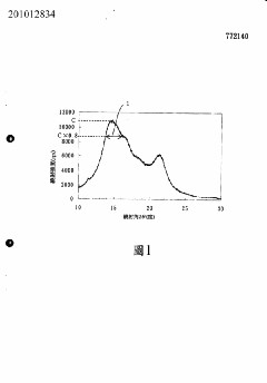
Optic thin film
PatentInactiveTW201012834A
Innovation
- Novel composition of propylene system co-polymer using 1-butene and propylene monomers for optic thin films.
- Unique layered structure with specific lattice dimensions (a-axis > 6.70A, b-axis > 21.5A) determined by x-ray diffraction.
- Cost-effective thin film with superior optical homogeneity.
Manufacturing Process
The manufacturing process of polypropylene thin films for optoelectronic devices involves several critical steps and considerations. The process typically begins with the selection of high-quality polypropylene resin, which is then melted and extruded through a die to form a thin sheet. This initial sheet undergoes a series of stretching and orientation processes to achieve the desired thickness and optical properties.
One of the key techniques in this process is biaxial orientation, where the film is stretched in both the machine direction and transverse direction. This orientation process significantly enhances the film's mechanical strength, optical clarity, and barrier properties. The stretching is usually performed at temperatures slightly below the melting point of polypropylene to ensure optimal molecular alignment.
Following the orientation process, the film may undergo surface treatments to improve its adhesion properties and compatibility with various coatings or functional layers. These treatments can include corona discharge, plasma treatment, or chemical priming. Such modifications are crucial for ensuring proper bonding between the polypropylene film and subsequent layers in optoelectronic devices.
The next stage often involves the application of specialized coatings or the deposition of functional materials. This can be achieved through various methods such as vacuum deposition, sputtering, or solution-based coating techniques. The choice of deposition method depends on the specific requirements of the optoelectronic device being manufactured.
Quality control is a critical aspect throughout the manufacturing process. Inline monitoring systems are employed to continuously assess film thickness, optical properties, and surface quality. Advanced inspection techniques, such as optical microscopy and spectroscopic analysis, are used to detect any defects or inconsistencies in the film structure.
The final steps in the manufacturing process typically involve cutting the film to the required dimensions and packaging it for transportation or further processing. Special care is taken to maintain the cleanliness and integrity of the film, often requiring cleanroom conditions and specialized handling equipment.
Continuous research and development efforts are focused on improving the manufacturing process to enhance the performance of polypropylene thin films in optoelectronic applications. This includes exploring new additives to improve optical properties, developing more efficient orientation techniques, and investigating novel surface modification methods to expand the range of potential applications in the optoelectronic industry.
Environmental Impact
The environmental impact of polypropylene thin films in optoelectronic devices is a crucial consideration in the development and adoption of this technology. Polypropylene, a thermoplastic polymer, offers several advantages in terms of sustainability compared to traditional materials used in optoelectronic applications.
One of the primary environmental benefits of polypropylene thin films is their potential for recyclability. Unlike many other materials used in electronic devices, polypropylene can be easily recycled and repurposed, reducing the overall waste generated by the optoelectronics industry. This characteristic aligns with the growing global emphasis on circular economy principles and sustainable manufacturing practices.
Furthermore, the production of polypropylene thin films generally requires less energy compared to the manufacturing of alternative materials such as glass or certain metals. This lower energy consumption translates to reduced carbon emissions throughout the production process, contributing to a smaller carbon footprint for optoelectronic devices incorporating these films.
The lightweight nature of polypropylene thin films also offers indirect environmental benefits. When used in portable electronic devices, these films can contribute to overall weight reduction, potentially leading to improved energy efficiency during device operation and transportation. This can result in lower energy consumption and reduced greenhouse gas emissions over the lifecycle of the product.
However, it is important to note that the environmental impact of polypropylene thin films is not entirely positive. The production of polypropylene, like other plastics, relies on fossil fuel resources. This dependency raises concerns about long-term sustainability and the need for alternative, bio-based sources for polymer production.
Additionally, while polypropylene is recyclable, the actual recycling rates for thin films used in electronic devices remain relatively low. This is partly due to the challenges in separating and collecting these films from complex electronic assemblies. Improving the design for disassembly and establishing more efficient recycling systems for electronic waste are crucial steps in maximizing the environmental benefits of polypropylene thin films.
The durability and chemical resistance of polypropylene thin films present both advantages and challenges from an environmental perspective. On one hand, these properties can lead to longer-lasting devices, reducing the frequency of replacement and associated waste. On the other hand, if not properly managed at the end of their life cycle, these films may persist in the environment for extended periods.
In conclusion, while polypropylene thin films offer several environmental advantages in optoelectronic applications, realizing their full potential for sustainability requires a holistic approach. This includes optimizing production processes, improving recycling infrastructure, and considering the entire lifecycle of devices incorporating these films. As research and development in this field progress, it is essential to continually assess and mitigate the environmental impacts to ensure that the benefits of this technology are maximized while minimizing its ecological footprint.
Unlock deeper insights with Patsnap Eureka Quick Research — get a full tech report to explore trends and direct your research. Try now!
Generate Your Research Report Instantly with AI Agent
Supercharge your innovation with Patsnap Eureka AI Agent Platform!