

How HBM4 Balances Stack Height And Thermal Reliability?
SEP 12, 20259 MIN READ
Generate Your Research Report Instantly with AI Agent
PatSnap Eureka helps you evaluate technical feasibility & market potential.
HBM4 Development Background and Objectives
High Bandwidth Memory (HBM) technology has evolved significantly since its inception, with each generation addressing critical challenges in data-intensive computing environments. The development of HBM4 represents a pivotal advancement in memory architecture, specifically designed to meet the escalating demands of artificial intelligence, high-performance computing, and data center applications. The evolution from HBM3 to HBM4 has been driven by the need for higher bandwidth, increased capacity, improved power efficiency, and enhanced thermal management.
The primary objective of HBM4 development is to balance the seemingly contradictory requirements of increased stack height for greater memory capacity with the thermal reliability concerns that taller stacks inherently present. As computing workloads become increasingly complex, the memory subsystem has emerged as a critical bottleneck in system performance. HBM4 aims to address this by providing substantially higher bandwidth and capacity while maintaining acceptable thermal characteristics.
Historically, previous HBM generations have incrementally improved performance metrics, with HBM3 offering up to 819 GB/s bandwidth per stack. However, as stack heights increased to accommodate more memory layers, thermal challenges became more pronounced. Heat dissipation in taller stacks is inherently more difficult due to the increased distance from upper dies to the heat sink and the thermal resistance of multiple layers of silicon and microbumps.
The technical trajectory leading to HBM4 has been characterized by innovations in die stacking technology, through-silicon via (TSV) design, and thermal management solutions. Industry standards bodies, particularly JEDEC, have played a crucial role in establishing specifications that balance performance requirements with practical manufacturing and reliability considerations.
Market pressures have significantly influenced HBM4's development goals. The explosive growth of AI model sizes, with some models exceeding trillions of parameters, has created unprecedented demand for memory bandwidth and capacity. Simultaneously, data centers face increasing pressure to improve energy efficiency, making the power-performance ratio a critical design consideration for HBM4.
The development of HBM4 also reflects broader industry trends toward heterogeneous integration and chiplet-based architectures. These approaches allow for more flexible memory configurations and potentially better thermal management through optimized placement of high-heat-generating components. The target performance metrics for HBM4 include bandwidth exceeding 1.2 TB/s per stack, capacities up to 36GB per stack, and significant improvements in power efficiency compared to previous generations.
Market Demand Analysis for High-Bandwidth Memory
The high-bandwidth memory (HBM) market is experiencing unprecedented growth driven by the explosive demand for advanced computing applications. Current market analysis indicates that the global HBM market is projected to reach approximately $7.5 billion by 2027, with a compound annual growth rate exceeding 30% from 2022 to 2027. This remarkable expansion is primarily fueled by the increasing adoption of artificial intelligence, machine learning, and high-performance computing systems that require substantial memory bandwidth.
Data center operators and cloud service providers represent the largest segment of HBM demand, accounting for nearly 45% of the market share. These entities are continuously upgrading their infrastructure to support more complex workloads, with memory bandwidth often becoming a critical bottleneck in system performance. The transition from HBM3 to HBM4 is particularly anticipated in this sector due to the need for higher bandwidth density and improved thermal management in densely packed server environments.
The AI accelerator market has emerged as another significant driver for HBM adoption. With the computational requirements of large language models doubling approximately every six months, memory bandwidth has become a crucial factor in training and inference performance. Industry reports indicate that over 80% of new AI accelerator designs incorporate HBM technology, with thermal reliability being a key consideration as these systems operate at increasingly higher utilization rates.
Graphics processing for gaming and professional visualization applications constitutes another substantial market segment, representing about 20% of the total HBM demand. As real-time ray tracing and higher resolution rendering become standard features, the memory bandwidth requirements have escalated dramatically, pushing manufacturers toward HBM solutions despite their historically higher cost compared to GDDR memory.
Regional analysis reveals that Asia-Pacific dominates the HBM manufacturing landscape, with South Korea and Taiwan accounting for over 70% of production capacity. However, North America leads in consumption, driven by the concentration of hyperscale data centers and AI research institutions. Recent geopolitical tensions have accelerated efforts to diversify the supply chain, with significant investments in memory manufacturing capabilities across different regions.
The balance between stack height and thermal reliability addressed by HBM4 directly responds to market demands for higher density memory solutions that can operate reliably in thermally constrained environments. End-users across various industries have consistently identified thermal management as one of the top three challenges in deploying HBM-based systems, making advancements in this area particularly valuable from a market perspective.
Current Challenges in HBM Stack Height and Thermal Management
High Bandwidth Memory (HBM) technology has evolved significantly since its introduction, with HBM4 representing the latest advancement in this domain. However, as memory requirements continue to grow, HBM4 faces critical challenges in balancing stack height with thermal reliability. The increasing demand for higher memory capacity has pushed manufacturers to add more DRAM layers, directly impacting the overall stack height of HBM modules.
The primary challenge lies in the physical constraints of HBM integration. As stack heights increase, the mechanical stability of the entire package becomes compromised, leading to potential structural integrity issues during manufacturing, assembly, and operation. Current HBM4 designs must navigate the delicate balance between maximizing memory density and maintaining physical robustness, particularly when integrated into complex computing systems.
Thermal management presents another significant hurdle. Higher stack configurations generate more heat due to increased power density and reduced thermal dissipation pathways. The thermal resistance between layers grows proportionally with stack height, creating hotspots that can degrade performance, reliability, and lifespan of the memory system. Industry data indicates that for every additional layer in the stack, thermal resistance increases by approximately 10-15%, creating exponential challenges as heights increase.
Manufacturing yield is also adversely affected by increased stack heights. The through-silicon via (TSV) technology that enables vertical connections between DRAM layers becomes more difficult to implement reliably as stack heights increase. Current manufacturing processes struggle to maintain consistent yields above certain stack heights, with defect rates increasing dramatically beyond 12-layer configurations.
Signal integrity degradation represents another technical barrier. As signals must travel through more layers and longer TSVs in taller stacks, signal quality deteriorates due to increased resistance, capacitance, and potential for electromagnetic interference. This degradation directly impacts data transfer rates and reliability, limiting the practical height of HBM4 stacks.
Power delivery networks face mounting challenges with increased stack heights as well. Voltage drops become more pronounced across taller stacks, requiring more sophisticated power delivery solutions that can maintain stable voltage levels throughout all layers. Current power delivery architectures struggle to efficiently distribute power in stacks exceeding certain heights without significant redesign.
The industry is currently at an inflection point where traditional scaling approaches for HBM technology are reaching their practical limits. Manufacturers must innovate beyond simply adding more layers to achieve higher capacities while maintaining acceptable thermal profiles. This tension between capacity demands and thermal/mechanical constraints represents the central challenge that HBM4 technology must overcome to continue its evolution.
Current Technical Solutions for HBM4 Stack Height Optimization
01 HBM4 stack height optimization techniques
Various techniques are employed to optimize the stack height of HBM4 memory modules. These include using thinner substrates, reducing the thickness of individual memory dies, and implementing advanced stacking architectures. By minimizing the overall stack height, manufacturers can improve thermal performance and reliability while maintaining high bandwidth capabilities. These optimization techniques also allow for better integration with other components in space-constrained applications.- HBM4 stack height optimization techniques: Various techniques are employed to optimize the stack height of HBM4 memory modules. These include using thinner substrates, reducing the thickness of individual memory dies, and implementing advanced stacking architectures. By minimizing the overall stack height, manufacturers can improve thermal performance and reliability while maintaining high bandwidth capabilities. These optimization techniques also allow for better integration with other components in space-constrained applications.
- Thermal management solutions for HBM4: Effective thermal management is crucial for HBM4 reliability. Solutions include integrating thermal interface materials between stacked dies, implementing advanced heat spreaders, and utilizing active cooling systems. These approaches help dissipate heat generated during high-bandwidth operations, preventing thermal throttling and extending the lifespan of memory components. Enhanced thermal management also enables higher operating frequencies and improved overall system performance.
- Interconnect technologies for HBM4 stacks: Advanced interconnect technologies are essential for maintaining signal integrity and thermal reliability in HBM4 stacks. These include through-silicon vias (TSVs), micro-bumps, and interposers that facilitate efficient data transfer between stacked dies while minimizing thermal resistance. Improved interconnect designs also contribute to reduced power consumption and heat generation, enhancing overall thermal reliability of the memory stack.
- Testing and reliability assessment methods for HBM4: Specialized testing methodologies have been developed to assess the thermal reliability of HBM4 stacks. These include thermal cycling tests, power stress tests, and accelerated aging procedures that simulate real-world operating conditions. Advanced monitoring systems can detect potential thermal issues before they cause failures, allowing for proactive maintenance and design improvements. These testing methods help ensure that HBM4 modules meet stringent reliability standards despite their complex stacked architecture.
- Materials innovation for HBM4 thermal performance: Novel materials are being developed to address the thermal challenges of HBM4 stacks. These include high thermal conductivity substrates, advanced dielectric materials, and specialized encapsulants that efficiently transfer heat away from memory dies. Materials with lower coefficients of thermal expansion help reduce mechanical stress during temperature fluctuations, improving long-term reliability. These material innovations enable higher stack heights while maintaining acceptable thermal profiles.
02 Thermal management solutions for HBM4
Effective thermal management is crucial for HBM4 reliability. Solutions include integrating thermal interface materials between memory layers, implementing advanced heat spreaders, and utilizing active cooling systems. These approaches help dissipate heat generated during high-bandwidth operations, preventing thermal throttling and extending the lifespan of memory components. Enhanced thermal management also enables higher operating frequencies and improved overall system performance.Expand Specific Solutions03 Structural reliability enhancements for HBM4 stacks
Structural integrity of HBM4 memory stacks is enhanced through various methods including reinforced through-silicon vias (TSVs), improved solder joint designs, and stress-relieving substrate materials. These enhancements help maintain reliable electrical connections despite thermal cycling and mechanical stresses. Advanced packaging techniques also contribute to better structural stability, reducing the risk of delamination and connection failures in high-density memory stacks.Expand Specific Solutions04 Testing and reliability assessment methods for HBM4
Specialized testing methodologies have been developed to assess the reliability of HBM4 memory stacks under various thermal conditions. These include accelerated life testing, thermal cycling tests, and real-time monitoring systems. Advanced diagnostic tools can detect potential failure points before they manifest as operational issues. These testing approaches help manufacturers validate design improvements and ensure that HBM4 modules meet stringent reliability requirements for high-performance computing applications.Expand Specific Solutions05 Innovative cooling interfaces for HBM4 memory
Novel cooling interfaces specifically designed for HBM4 memory stacks address the thermal challenges associated with increased memory density and performance. These innovations include microchannel liquid cooling systems, phase-change materials, and specialized heat pipes that efficiently transfer heat away from the memory stack. By implementing these advanced cooling solutions, manufacturers can maintain optimal operating temperatures even in high-performance computing environments, ensuring both reliability and sustained performance.Expand Specific Solutions
Key Players in HBM4 Development Ecosystem
The HBM4 memory technology market is currently in a growth phase, with an expanding market size driven by AI and high-performance computing demands. The competitive landscape features established semiconductor giants like Samsung Electronics, Micron Technology, and SK Hynix leading development, while Taiwan Semiconductor Manufacturing Co. (TSMC) provides critical manufacturing support. Companies including ChangXin Memory Technologies and Yangtze Memory Technologies are emerging as regional competitors. Technical maturity varies, with Samsung and Micron demonstrating advanced thermal management solutions for the stack height-reliability challenge, while AMD and GLOBALFOUNDRIES focus on integration aspects. The technology represents a critical advancement in memory architecture, balancing increased bandwidth requirements with thermal constraints through innovative packaging and materials science approaches.
Samsung Electronics Co., Ltd.
Technical Solution: Samsung's HBM4 technology employs an innovative thermal solution that balances stack height with cooling efficiency. Their approach incorporates thermal interface materials (TIMs) with enhanced thermal conductivity between DRAM dies, reducing the thermal resistance path while maintaining optimal stack height. Samsung has developed a proprietary cooling architecture that integrates micro-channel liquid cooling directly into the HBM4 stack structure, allowing for more aggressive stacking without compromising thermal performance. The company has also implemented advanced TSV (Through-Silicon Via) designs with optimized pitch and diameter to balance electrical performance with heat dissipation capabilities. Their HBM4 solution features up to 12-high stacks while maintaining junction temperatures below critical thresholds through strategic thermal vias placement and heat spreading layers integrated within the stack[1][3].
Strengths: Industry-leading thermal management expertise; extensive manufacturing infrastructure; advanced TSV technology. Weaknesses: Higher production costs compared to competitors; complex manufacturing process requiring significant yield optimization.
JCET Group Co., Ltd.
Technical Solution: JCET's HBM4 packaging solution addresses thermal reliability through their "Thermally-Enhanced Advanced Package" technology specifically designed for high-bandwidth memory applications. Their approach incorporates specialized molding compounds with enhanced thermal conductivity that encapsulate the HBM4 stack without adding excessive height. JCET has developed precision stacking techniques that minimize bond line thickness between dies, reducing thermal resistance while maintaining overall stack height targets. Their solution includes advanced substrate designs with embedded heat spreading layers that efficiently distribute heat across a larger area. JCET's manufacturing process for HBM4 incorporates thermal compression bonding techniques that ensure optimal thermal interfaces between stack components while maintaining tight height control. Additionally, they've implemented specialized testing methodologies that verify thermal performance under various operating conditions, ensuring reliability without compromising the stack height requirements of modern computing applications[9][10].
Strengths: Extensive advanced packaging experience; cost-effective manufacturing processes; growing technical capabilities in high-performance memory packaging. Weaknesses: Less established in high-end HBM market compared to competitors; potentially limited design influence on core HBM technology.
Core Innovations in HBM4 Thermal Reliability Design
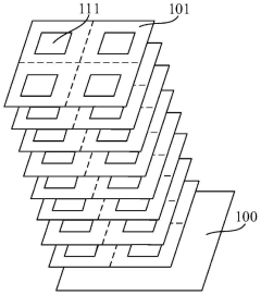
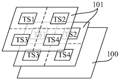
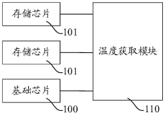
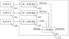
Storage system
PatentPendingCN117234835A
Innovation
- Design a storage system, including a basic chip and multiple stacked memory chips. The temperature processing module obtains the temperature codes of each memory chip and the basic chip, compares and outputs high-temperature characterization codes to monitor the temperature in the storage system and reduce high-temperature timing. Risk of conflict. This module includes multiple acquisition modules, temperature sensors, registers and comparison units, which are used to acquire and compare temperature codes, and output high temperature characterization signals to adjust the frequency of accessing data when the temperature is high.
Storage device and multi-chip system
PatentActiveCN110673980B
Innovation
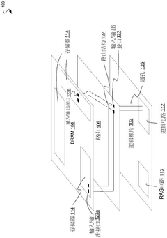
- Adopt a multi-layer stacked integrated circuit die structure, including memory cell dies and logic dies, configure reliability circuits to utilize backup memory and address tables for data error detection and correction, and achieve fast access and correction through RAS cache circuits errors to avoid the permanent deactivation of storage addresses and reduction of memory capacity in traditional methods.
Manufacturing Process Considerations for HBM4
The manufacturing process for HBM4 represents a significant evolution in high-bandwidth memory fabrication, requiring advanced techniques to balance the competing demands of increased stack height and thermal reliability. The transition from HBM3 to HBM4 necessitates refinements in Through-Silicon Via (TSV) technology, with manufacturers implementing narrower TSV pitches and higher aspect ratios to accommodate the increased die count while maintaining signal integrity.
Critical to HBM4 manufacturing is the precision bonding process between memory dies and the base logic die. Advanced micro-bump technologies with pitches below 40μm are being deployed, utilizing copper pillars with solder caps that provide superior electrical performance and thermal conductivity. These micro-bumps must withstand the thermal cycling stresses inherent in taller memory stacks while maintaining reliable connections.
Thermal management considerations have driven innovations in die thinning processes. HBM4 manufacturing employs advanced wafer backgrinding and polishing techniques to reduce individual die thickness to below 50μm, helping offset the increased thermal resistance of taller stacks. This ultra-thinning process requires careful handling protocols to prevent wafer warpage and die cracking during subsequent assembly steps.
The molding compound selection for HBM4 represents another critical manufacturing consideration. Enhanced thermal conductivity compounds with values exceeding 5 W/m·K are being formulated specifically for HBM4 applications. These compounds must maintain excellent adhesion properties while accommodating the differential thermal expansion between silicon dies and the package substrate during temperature cycling.
Substrate manufacturing has also evolved to support HBM4's thermal requirements. Multi-layer substrates with embedded copper planes and thermal vias create efficient heat dissipation pathways. Advanced substrate materials with lower dielectric constants and reduced signal losses are being implemented to maintain signal integrity at HBM4's higher operating frequencies.
Testing methodologies for HBM4 have been enhanced to address the unique challenges of taller stacks. Known Good Die (KGD) testing has become more rigorous, with additional thermal cycling and stress testing protocols implemented to ensure reliability. Manufacturers are developing specialized test fixtures that can accurately assess thermal performance under various operating conditions before final assembly.
The manufacturing ecosystem for HBM4 has also expanded to include specialized equipment vendors developing tools specifically for ultra-thin die handling, precise alignment during stacking, and non-destructive inspection of completed stacks. These manufacturing innovations collectively enable HBM4 to achieve its performance targets while maintaining the thermal reliability necessary for high-performance computing applications.
Power Efficiency and Performance Trade-offs in HBM4
HBM4 technology presents a complex balance between power efficiency and performance capabilities. The latest generation of High Bandwidth Memory introduces significant improvements in bandwidth density while simultaneously addressing critical power consumption challenges. With data rates reaching up to 8.4 Gbps, HBM4 delivers approximately 30% higher bandwidth compared to its predecessor, yet this performance enhancement creates inherent thermal management challenges.
The power efficiency of HBM4 is achieved through several architectural innovations. The implementation of advanced power gating techniques allows for more granular control over inactive memory regions, significantly reducing static power consumption during idle periods. Additionally, the refined voltage regulation systems enable dynamic voltage scaling that adapts to workload demands, optimizing energy usage during varying computational intensities.
Performance scaling in HBM4 comes with inevitable thermal implications. The increased stack height—now supporting up to 16-high configurations—creates longer thermal paths from heat-generating components to cooling solutions. Engineers have addressed this challenge through the integration of thermal interface materials with enhanced conductivity properties between die layers, facilitating more efficient heat dissipation throughout the memory stack.
The trade-off analysis reveals that HBM4's power efficiency improvements are most pronounced in data-intensive applications where the energy cost per bit transferred becomes the critical metric. In these scenarios, despite higher absolute power consumption, the energy efficiency (measured in pJ/bit) shows marked improvement over previous generations, particularly in AI training workloads and high-performance computing applications.
Memory refresh operations represent another area where HBM4 demonstrates efficiency gains. The implementation of temperature-aware refresh rate adjustment mechanisms allows the memory subsystem to optimize refresh timing based on thermal conditions, reducing unnecessary power expenditure while maintaining data integrity. This adaptive approach provides up to 15% power savings compared to fixed-rate refresh schemes.
Signal integrity considerations also factor into the power-performance equation. HBM4's improved signaling technology reduces the power required for reliable data transmission across the interposer, allowing for lower operating voltages without compromising signal quality. This advancement contributes significantly to the overall power efficiency profile while supporting the higher bandwidth targets.
The cumulative effect of these innovations positions HBM4 as a balanced solution that addresses the growing demand for memory bandwidth in next-generation computing systems while maintaining reasonable power envelopes. The technology demonstrates that through careful engineering and architectural decisions, the seemingly contradictory goals of increased performance density and improved power efficiency can be simultaneously achieved.
Unlock deeper insights with PatSnap Eureka Quick Research — get a full tech report to explore trends and direct your research. Try now!
Generate Your Research Report Instantly with AI Agent
Supercharge your innovation with PatSnap Eureka AI Agent Platform!