

How HBM4 Improves Interposer Routing Efficiency And Density?
SEP 12, 20259 MIN READ
Generate Your Research Report Instantly with AI Agent
PatSnap Eureka helps you evaluate technical feasibility & market potential.
HBM4 Technology Evolution and Objectives
High Bandwidth Memory (HBM) technology has evolved significantly since its inception, with each generation bringing substantial improvements in bandwidth, capacity, and energy efficiency. The journey from HBM1 to HBM4 represents a continuous pursuit of meeting the escalating demands of data-intensive applications such as artificial intelligence, high-performance computing, and graphics processing. HBM4, as the latest iteration, marks a pivotal advancement in addressing the critical challenges of interposer routing efficiency and density.
The evolution of HBM technology began with HBM1 in 2013, offering bandwidth of approximately 128 GB/s per stack. HBM2 followed in 2016, doubling the bandwidth to about 256 GB/s per stack. HBM2E, introduced in 2018, further enhanced performance to around 460 GB/s per stack. HBM3, launched in 2021, pushed the boundaries to achieve up to 819 GB/s per stack. Now, HBM4 aims to deliver unprecedented bandwidth exceeding 1 TB/s per stack, representing an exponential growth trajectory in memory performance.
A primary objective of HBM4 development is to overcome the routing congestion challenges that have plagued previous generations. As data rates increased, the complexity and density of interposer routing became significant bottlenecks, limiting the scalability of HBM implementations. HBM4 addresses this through innovative architectural changes that fundamentally rethink how signals are routed between the memory dies and the host processor.
Another critical goal for HBM4 is enhancing energy efficiency. Previous generations faced challenges in balancing performance gains with power consumption. HBM4 aims to deliver substantial bandwidth improvements while maintaining or even reducing the energy per bit transferred, a crucial factor for deployment in power-constrained environments such as data centers and mobile high-performance computing platforms.
The industry trend toward chiplet-based architectures has also influenced HBM4's development objectives. With system designers increasingly adopting disaggregated chip designs, HBM4 seeks to provide more flexible integration options that can accommodate diverse chiplet configurations while maximizing routing efficiency across the interposer.
Manufacturing scalability represents another key objective for HBM4. Previous HBM generations faced yield challenges due to the complexity of stacking multiple dies and implementing through-silicon vias (TSVs). HBM4 aims to introduce design innovations that improve manufacturability while enabling higher capacity and performance, ensuring that the technology can be produced at scale to meet growing market demands.
Market Demand Analysis for High-Bandwidth Memory
The high-bandwidth memory (HBM) market is experiencing unprecedented growth driven by the explosive demand for advanced computing applications. Current market analysis indicates that the global HBM market is projected to reach $3.6 billion by 2025, with a compound annual growth rate exceeding 30% from 2020 to 2025. This remarkable expansion is primarily fueled by the increasing adoption of artificial intelligence, machine learning, and high-performance computing technologies across various industries.
Data centers represent the largest market segment for HBM technology, accounting for approximately 40% of the total market share. The rapid proliferation of cloud computing services and the growing need for processing massive datasets have created substantial demand for memory solutions that can deliver higher bandwidth with improved power efficiency. HBM technology addresses these requirements effectively, making it an essential component in modern data center architectures.
The graphics processing market follows closely as the second-largest consumer of HBM technology. Advanced graphics applications, particularly in gaming, virtual reality, and professional visualization, require memory solutions capable of handling increasingly complex graphical workloads. The transition from GDDR memory to HBM in high-end graphics cards has been accelerating, with major GPU manufacturers incorporating HBM in their flagship products.
Artificial intelligence and machine learning applications have emerged as the fastest-growing segment for HBM technology. Training sophisticated neural networks demands enormous memory bandwidth to process vast datasets efficiently. Industry reports indicate that AI accelerator chips with HBM memory can achieve performance improvements of up to 300% compared to traditional memory architectures, significantly reducing model training time and operational costs.
The automotive sector represents an emerging market for HBM technology, particularly with the advancement of autonomous driving systems. These systems require real-time processing of sensor data from multiple sources, creating demand for high-bandwidth, low-latency memory solutions. Industry forecasts suggest that the automotive HBM market will grow at a CAGR of approximately 45% between 2021 and 2026.
Geographically, North America currently leads the HBM market with approximately 35% market share, followed by Asia-Pacific at 32% and Europe at 25%. However, the Asia-Pacific region is expected to witness the highest growth rate over the next five years, driven by the expanding semiconductor manufacturing capabilities in countries like South Korea, Taiwan, and China.
The transition from HBM3 to HBM4 is anticipated to accelerate market growth further, as HBM4's improved interposer routing efficiency and density directly address the performance bottlenecks in current memory architectures. Industry surveys indicate that 78% of high-performance computing system designers plan to adopt HBM4 in their next-generation products, highlighting the strong market demand for this technology advancement.
Current Interposer Routing Challenges and Limitations
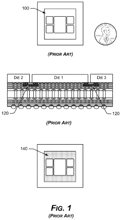
Interposer technology has become a critical component in advanced packaging solutions, particularly for high-bandwidth memory (HBM) integration. However, current interposer designs face significant routing challenges that limit their efficiency and scalability. The primary constraint stems from the increasing pin count and decreasing pitch requirements of modern HBM implementations, creating a routing congestion bottleneck at the interposer level.
Traditional silicon interposers typically utilize a redistribution layer (RDL) approach with limited metal layers, resulting in complex routing patterns that must navigate between thousands of microbumps. As HBM stacks have evolved from HBM1 through HBM3E, the microbump pitch has decreased from 50μm to approximately 40μm, while simultaneously increasing the total number of connections. This combination has created exponentially more difficult routing scenarios.
Signal integrity issues represent another major limitation in current interposer designs. As data rates have increased to support bandwidth demands, maintaining signal quality across the interposer has become increasingly challenging. Crosstalk between adjacent traces, impedance matching complications, and power delivery network (PDN) constraints all contribute to performance degradation in existing solutions.
Manufacturing yield concerns also plague current interposer technologies. The large silicon interposer area required for HBM integration results in higher defect probabilities compared to standard chip manufacturing. This directly impacts production costs and scalability, particularly as system designers seek to integrate more HBM stacks per package.
Thermal management presents additional complications in current interposer designs. The dense routing channels create heat dissipation challenges, potentially leading to performance throttling and reliability concerns in high-performance computing applications. The thermal interface between HBM stacks, the interposer, and the base die requires careful consideration that often conflicts with optimal routing strategies.
Power delivery network (PDN) design represents a significant routing challenge in current interposers. The high current requirements of HBM interfaces necessitate substantial power and ground connections, which compete for routing resources with high-speed data signals. This competition often forces design compromises that limit either power delivery robustness or signal routing density.
Test access and repairability also suffer under current interposer routing constraints. The dense interconnect patterns leave minimal space for test structures, making fault isolation and quality assurance more difficult. This limitation becomes increasingly problematic as system complexity grows with each HBM generation.
The economic implications of these technical limitations are substantial. Current interposer manufacturing processes require specialized equipment and precise fabrication techniques, resulting in high production costs that scale with interposer size and complexity. These factors collectively create a technological ceiling that the industry must overcome to enable the next generation of high-performance computing systems.
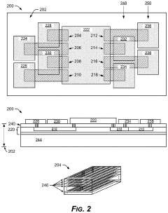
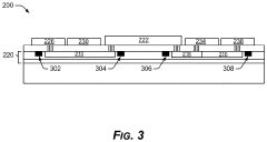
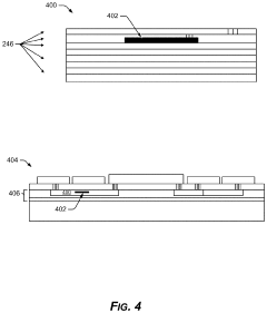
HBM4 Routing Efficiency Solutions and Implementations
01 Interposer design for high-density routing
Advanced interposer designs enable high-density routing for HBM4 applications by utilizing multi-layer structures with optimized trace layouts. These interposers incorporate fine-pitch interconnects and specialized routing algorithms to maximize the number of signal paths while minimizing crosstalk and signal degradation. The designs often feature through-silicon vias (TSVs) arranged in strategic patterns to facilitate efficient vertical connections between layers, significantly increasing routing density compared to traditional substrate technologies.- Interposer design for high-density routing: Advanced interposer designs enable high-density routing for HBM4 applications. These designs incorporate multiple routing layers with optimized trace widths and spacing to maximize the number of connections between the HBM memory and processor. The interposer structure serves as a critical interface that allows for efficient signal transmission while maintaining signal integrity at high frequencies, which is essential for HBM4 performance.
- Through-silicon via (TSV) optimization: Through-silicon vias (TSVs) are optimized in HBM4 interposers to improve routing efficiency and density. Advanced TSV designs feature reduced pitch, optimized aspect ratios, and improved metallization techniques to enhance electrical performance and reliability. These optimizations allow for more efficient vertical connections through the interposer, enabling higher bandwidth and better thermal management in HBM4 memory systems.
- Thermal management solutions for high-density interposers: Thermal management is critical for maintaining the performance and reliability of high-density HBM4 interposers. Innovative cooling solutions include integrated heat spreaders, thermal vias, and specialized materials with high thermal conductivity. These solutions help dissipate heat generated by the dense routing pathways and multiple memory stacks, preventing thermal-related performance degradation and ensuring stable operation of the HBM4 memory system.
- Advanced materials for interposer fabrication: Novel materials are employed in HBM4 interposer fabrication to enhance routing efficiency and density. These materials include low-loss dielectrics, high-conductivity metals, and specialized polymers that improve signal integrity while allowing for finer line widths and spacing. The use of these advanced materials enables higher routing density, reduced signal loss, and improved electrical performance in HBM4 memory systems.
- Design automation and optimization techniques: Sophisticated design automation and optimization techniques are employed to maximize routing efficiency in HBM4 interposers. These include advanced algorithms for trace routing, automated design rule checking, and simulation tools that optimize signal integrity and power distribution. Machine learning approaches are also being implemented to identify optimal routing patterns and configurations, resulting in higher routing density and improved overall system performance.
02 Thermal management solutions for high-density interposers
Thermal management is critical for HBM4 interposers with high routing density. Innovative cooling solutions include embedded thermal vias, integrated heat spreaders, and specialized materials with enhanced thermal conductivity. These approaches help dissipate heat generated by densely packed interconnects and active components, preventing performance degradation and reliability issues. Advanced thermal simulation techniques are employed during design to identify and address potential hotspots in high-density routing areas.Expand Specific Solutions03 Advanced manufacturing techniques for fine-pitch routing
Manufacturing techniques specifically developed for fine-pitch routing in HBM4 interposers include precision lithography, advanced etching processes, and specialized deposition methods. These techniques enable the creation of ultra-narrow traces and spaces, significantly increasing routing efficiency. Novel approaches such as semi-additive processing and laser-assisted patterning allow for the fabrication of complex routing structures with minimal defects, enhancing overall yield and reliability of high-density interposers.Expand Specific Solutions04 Signal integrity optimization for high-speed channels
Signal integrity optimization is essential for maintaining performance in high-density HBM4 interposers. Techniques include impedance matching, crosstalk reduction through shielding structures, and specialized trace geometries that minimize reflections and signal distortion. Advanced simulation tools are used to model and optimize high-speed channels, ensuring reliable data transmission even with closely packed routing. Differential pair routing strategies and ground plane designs are carefully engineered to maintain signal quality at increased routing densities.Expand Specific Solutions05 Novel materials and structures for enhanced routing efficiency
Innovative materials and structural designs significantly improve routing efficiency in HBM4 interposers. These include low-loss dielectric materials, high-conductivity metals for traces, and novel laminate structures that enable more routing layers in a given thickness. Some designs incorporate embedded passive components to free up surface routing space. Hierarchical routing architectures with specialized regions for different signal types help maximize overall routing efficiency while maintaining performance requirements for critical paths.Expand Specific Solutions
Key Industry Players in HBM and Interposer Technologies
The HBM4 technology market is currently in a growth phase, with increasing demand for high-bandwidth memory solutions in AI, data centers, and high-performance computing applications. The competitive landscape is dominated by established semiconductor manufacturers like Samsung Electronics, Micron Technology, and SK Hynix, who are investing heavily in HBM4 development. The market size is projected to expand significantly as data-intensive applications proliferate, with estimates suggesting a multi-billion dollar opportunity by 2025. From a technical maturity perspective, companies like TSMC, Intel, and AMD are advancing interposer routing technologies to maximize HBM4's potential, while Synopsys and Rambus are developing supporting IP solutions. Memory manufacturers and foundries are collaborating to overcome the complex technical challenges of increasing routing efficiency while maintaining signal integrity across high-density interposers.
Samsung Electronics Co., Ltd.
Technical Solution: Samsung has pioneered significant advancements in HBM4 interposer routing efficiency through their innovative "Through-Silicon Via (TSV) Optimization" approach. Their technology implements a redesigned TSV arrangement that increases signal integrity while reducing crosstalk between channels. Samsung's HBM4 solution features an 8-high stack configuration with over 40,000 TSVs, enabling bandwidth exceeding 1.6TB/s per stack[1]. The company has implemented a novel interposer design with optimized trace routing that reduces signal path lengths by approximately 15% compared to previous generations. Their proprietary "Smart Routing Algorithm" dynamically allocates routing resources based on thermal and electrical constraints, significantly improving overall density. Samsung has also introduced advanced materials for their interposers, including silicon-based interposers with sub-micron routing capabilities that support the increased I/O density requirements of HBM4.
Strengths: Samsung's extensive manufacturing expertise allows for highly optimized production processes, resulting in higher yields and better cost efficiency. Their vertical integration from memory design to packaging gives them complete control over the entire HBM4 ecosystem. Weaknesses: Their proprietary approach may limit compatibility with some third-party systems, and the advanced manufacturing processes required for their optimized interposer designs demand significant capital investment.
Intel Corp.
Technical Solution: Intel has developed a comprehensive approach to HBM4 interposer routing through their "Embedded Multi-die Interconnect Bridge" (EMIB) technology, which they've evolved specifically for HBM4 applications. Intel's solution addresses interposer routing challenges by implementing a segmented interposer approach that places smaller silicon bridges only where high-density interconnects are required. For HBM4 integration, Intel has enhanced their EMIB technology with ultra-fine pitch interconnects (sub-35μm) and advanced routing algorithms that optimize signal integrity across the high-speed channels[2]. Their approach reduces the overall silicon interposer area by approximately 60% compared to traditional full interposer designs, while maintaining the necessary routing density for HBM4's increased bandwidth requirements. Intel has also implemented advanced power delivery networks within their interposer design that reduce voltage droop and improve signal integrity across the high-speed memory channels, enabling the full performance potential of HBM4 memory while minimizing power consumption.
Strengths: Intel's EMIB approach offers significant cost advantages over full silicon interposers while maintaining high performance. Their segmented design provides better yield management and thermal characteristics. Weaknesses: The segmented approach may introduce additional design complexity for some applications, and the technology requires precise alignment during manufacturing, potentially affecting production yields for the most advanced implementations.
Critical Innovations in HBM4 Interposer Design
Embedded organic interposer for high bandwidth
PatentPendingUS20210327851A1
Innovation
- Embedded organic interposers with thicker conductors and additional routing layers are embedded within the package core, providing more dielectric space and reducing the resistive-capacitive (RC) load to achieve higher bandwidth transmission, up to 20-60 GHz over longer spans.
Aggregation of multiple memory modules for a system-on-chip
PatentPendingUS20240403235A1
Innovation
- The integration of a buffer die with a shared memory interface on an interposer substrate allows multiple HBM modules to communicate with the SoC, reducing the need for individual memory interfaces and maintaining a compact SoC size while increasing memory capacity.


Thermal Management Considerations for High-Density HBM4 Systems
The increased routing density and efficiency of HBM4 introduces significant thermal management challenges that must be addressed for reliable system operation. As HBM4 stacks more memory dies with higher bandwidth capabilities, power density increases substantially, creating concentrated heat zones that can impact both performance and reliability.
Thermal considerations for HBM4 systems begin with the interposer design itself. The improved routing efficiency that enables higher bandwidth simultaneously creates more densely packed signal paths, which can impede heat dissipation through the interposer substrate. This necessitates advanced thermal modeling approaches that account for the three-dimensional heat flow characteristics unique to HBM4 implementations.
Heat dissipation strategies must evolve to address the thermal challenges of high-density HBM4 systems. Traditional cooling methods become insufficient as thermal density increases, requiring innovations such as integrated microchannel cooling, phase-change materials, and advanced thermal interface materials (TIMs) with higher thermal conductivity. These solutions must maintain compatibility with the fine-pitch interconnects that enable HBM4's routing efficiency advantages.
The thermal coupling between HBM4 stacks and processing elements presents another critical consideration. As interposer routing enables closer placement of memory and compute elements, thermal interactions become more pronounced. System designers must implement thermal isolation techniques while maintaining the electrical connectivity benefits that HBM4's improved routing efficiency provides.
Power management strategies become increasingly important in thermal management of HBM4 systems. Dynamic thermal management techniques, including adaptive refresh rates and intelligent power throttling, can help mitigate thermal issues during peak operation periods. These approaches must be carefully balanced against performance requirements to maintain the bandwidth advantages that HBM4 offers.
Reliability implications of thermal management decisions cannot be overlooked. The improved routing efficiency of HBM4 creates systems with higher functional density but potentially greater thermal vulnerability. Thermal cycling effects on microbumps, through-silicon vias (TSVs), and interposer routing must be thoroughly analyzed to ensure system longevity, particularly in applications with variable workloads that create frequent thermal fluctuations.
Testing methodologies for thermal performance must evolve alongside HBM4 technology. Traditional thermal testing approaches may not adequately capture the complex thermal interactions in densely routed HBM4 systems. Advanced infrared imaging, embedded thermal sensors, and computational fluid dynamics modeling become essential tools for validating thermal management solutions in these high-density memory systems.
Manufacturing Process Advancements for HBM4 Integration
The manufacturing processes for HBM4 integration represent a significant leap forward in semiconductor fabrication technology. Advanced silicon interposer manufacturing techniques have evolved to accommodate the increased routing density requirements of HBM4. The transition from traditional subtractive etching to semi-additive and fully additive processes has enabled the creation of finer line widths and spacing, critical for the higher interconnect density demanded by HBM4's architecture.
Through-Silicon Via (TSV) technology has undergone substantial refinement for HBM4 implementation. The aspect ratio of TSVs has been optimized to balance electrical performance with manufacturing yield. Newer TSV formation techniques employ laser drilling and advanced filling methods that reduce stress on the silicon substrate while improving electrical conductivity. These enhancements directly contribute to HBM4's ability to support higher bandwidth with improved signal integrity.
Advanced wafer thinning and handling methodologies have been developed specifically for HBM4 production. Ultra-precise grinding and polishing techniques now achieve consistent wafer thicknesses below 50 micrometers, enabling shorter TSV connections and reducing signal propagation delays. Temporary bonding materials with improved thermal stability support these thinner wafers through high-temperature processing steps without compromising structural integrity.
Micro-bump technology has evolved to accommodate HBM4's finer pitch requirements. The industry has transitioned from traditional solder bumps to copper pillar technology with pitches below 40 micrometers. Advanced underfill materials with optimized flow characteristics ensure void-free filling between these tightly spaced interconnects, enhancing both electrical performance and mechanical reliability of the HBM4 stack.
Precision die alignment and bonding processes have reached unprecedented accuracy levels for HBM4 integration. Automated optical inspection systems combined with advanced placement tools now achieve alignment accuracies below 1 micrometer. Thermal compression bonding techniques have been refined to create reliable interconnections while minimizing stress on the delicate interposer routing structures.
Quality control methodologies have been enhanced through non-destructive testing techniques specifically developed for HBM4 stacks. Advanced X-ray inspection systems with tomographic capabilities can detect sub-micron defects within the complex 3D structure. Electrical test methodologies have evolved to efficiently validate the thousands of interconnections present in HBM4 implementations, significantly improving manufacturing yield rates.
Unlock deeper insights with PatSnap Eureka Quick Research — get a full tech report to explore trends and direct your research. Try now!
Generate Your Research Report Instantly with AI Agent
Supercharge your innovation with PatSnap Eureka AI Agent Platform!