

How HBM4 Packaging Improves Yield And Mechanical Reliability?
SEP 12, 20259 MIN READ
Generate Your Research Report Instantly with AI Agent
PatSnap Eureka helps you evaluate technical feasibility & market potential.
HBM4 Packaging Evolution and Objectives
High Bandwidth Memory (HBM) technology has evolved significantly since its introduction, with each generation bringing substantial improvements in performance, capacity, and reliability. HBM4, the latest iteration in this evolution, represents a significant leap forward in addressing the growing demands of data-intensive applications such as artificial intelligence, high-performance computing, and advanced graphics processing. The development of HBM4 builds upon the foundations established by its predecessors—HBM1, HBM2, and HBM3—while introducing novel packaging techniques specifically designed to enhance yield and mechanical reliability.
The historical trajectory of HBM technology reveals a consistent focus on increasing bandwidth while managing power consumption and thermal challenges. HBM1, introduced in 2013, established the basic concept of stacked memory dies connected through through-silicon vias (TSVs). HBM2 followed in 2016 with doubled bandwidth and capacity, while HBM3 in 2021 further pushed performance boundaries with speeds exceeding 5 Gbps per pin.
HBM4 packaging technology aims to address several critical objectives that previous generations struggled to fully resolve. Primary among these is improving manufacturing yield—a persistent challenge due to the complexity of stacking multiple memory dies and connecting them to a base logic die. The intricate nature of these connections has historically resulted in higher defect rates compared to traditional memory technologies, directly impacting production costs and market availability.
Another key objective of HBM4 packaging innovation is enhancing mechanical reliability. As HBM stacks have grown taller with each generation to accommodate more memory capacity, they have become increasingly vulnerable to mechanical stresses during assembly, testing, and operation. These stresses can lead to microcracks, delamination between layers, and solder joint failures—all of which compromise long-term reliability and performance.
The technical evolution of HBM4 packaging also focuses on thermal management improvements. Previous HBM generations faced thermal challenges due to the dense stacking of memory dies, which created heat dissipation bottlenecks. HBM4 packaging techniques aim to optimize thermal pathways to maintain performance consistency under heavy computational loads while preventing thermal-induced mechanical failures.
Additionally, HBM4 packaging development targets improved signal integrity across the increasing number of interconnects. As data rates continue to climb, maintaining clean signal transmission becomes more challenging, requiring innovations in materials, geometries, and shielding techniques within the package structure.
These evolutionary objectives align with broader industry trends toward heterogeneous integration and chiplet-based architectures, positioning HBM4 as a critical enabling technology for next-generation computing systems that demand unprecedented memory bandwidth, capacity, and reliability.
Market Demand Analysis for Advanced Memory Solutions
The global market for advanced memory solutions is experiencing unprecedented growth, driven primarily by the exponential increase in data processing requirements across multiple sectors. High Bandwidth Memory (HBM) technology, particularly the forthcoming HBM4 standard, is positioned at the forefront of this demand curve. Current market analyses indicate that AI and machine learning applications are the primary drivers, with data centers requiring increasingly dense memory configurations to handle complex neural network training and inference operations.
The demand for HBM4 solutions stems from critical limitations in existing memory architectures. Traditional DRAM configurations can no longer satisfy the bandwidth requirements of advanced computing applications, creating a significant market gap that HBM4 aims to fill. Market research shows that AI accelerator cards, high-performance computing systems, and next-generation networking equipment represent the three largest potential markets for HBM4 technology.
From a geographical perspective, North America and East Asia dominate the demand landscape, with major cloud service providers and semiconductor manufacturers investing heavily in memory-intensive infrastructure. The automotive sector represents an emerging market segment, as advanced driver assistance systems and autonomous driving capabilities require substantial memory bandwidth for real-time processing of sensor data.
The economic value proposition of improved packaging yield and mechanical reliability in HBM4 cannot be overstated. Current HBM implementations face yield challenges due to the complexity of stacking multiple DRAM dies and connecting them via through-silicon vias (TSVs). These manufacturing difficulties translate directly to higher costs and limited availability, restricting market penetration.
Industry analysts project that improvements in HBM4 packaging yield could reduce production costs by a significant margin, potentially expanding the addressable market by making this technology accessible to mid-tier applications previously priced out of consideration. The enhanced mechanical reliability addresses another critical market concern: system longevity in high-value deployments where replacement costs extend beyond the components themselves.
Enterprise customers specifically highlight thermal management capabilities as a key purchasing factor, as current HBM solutions often require sophisticated cooling systems to maintain operational stability. The improved mechanical properties of HBM4 packaging promise better thermal conductivity and stress distribution, potentially reducing total cost of ownership for data center operators and other large-scale deployments.
Market forecasts suggest that the transition to HBM4 will accelerate adoption in edge computing applications, where space constraints and power limitations have previously prevented the use of high-bandwidth memory solutions. This represents a significant expansion of the potential market, particularly as 5G networks and IoT deployments continue to drive computational requirements closer to data sources.
Current Challenges in HBM Packaging Technology
Despite significant advancements in High Bandwidth Memory (HBM) technology, current HBM packaging faces several critical challenges that impact both yield and mechanical reliability. The complex 3D stacking architecture of HBM involves multiple silicon dies stacked vertically and interconnected with thousands of through-silicon vias (TSVs) and microbumps, creating inherent manufacturing difficulties that affect production yields.
One of the primary challenges is thermal management. As HBM stacks increase in height and density with each generation, heat dissipation becomes increasingly problematic. The concentrated heat can lead to thermal expansion mismatches between different materials in the package, causing mechanical stress that may result in warpage, delamination, or microbump failures. Current HBM3 implementations already struggle with these thermal issues, which become even more pronounced in HBM4 designs.
Microbump reliability presents another significant challenge. The microbumps connecting the stacked dies must maintain consistent electrical connections while withstanding thermal cycling and mechanical stress. As bump pitch decreases to accommodate higher bandwidth requirements, the risk of connection failures increases substantially. Current technologies face yield limitations due to the precision required for aligning and bonding these microscopic interconnects.
The interposer technology used in HBM packaging also presents yield challenges. Silicon interposers are expensive to manufacture and test, with defects in the interposer potentially rendering the entire package unusable. As HBM4 requires even more complex interposer designs with finer routing to support increased bandwidth, manufacturing yields face additional pressure.
Material selection and compatibility issues further complicate HBM packaging. The different coefficients of thermal expansion (CTE) between silicon dies, interposers, substrates, and molding compounds create mechanical stresses during temperature fluctuations. These stresses can lead to package warpage, die cracking, or interface delamination, all of which negatively impact reliability and yield.
Testing and quality assurance represent another major challenge. The highly integrated nature of HBM packages makes it difficult to test individual components after assembly. Known-good-die (KGD) testing becomes increasingly important but also more complex as stack heights increase and interconnect densities rise. The inability to effectively test intermediate assembly steps contributes to lower overall yields.
Manufacturing process control also presents significant challenges. The precise alignment required for die stacking, the uniform application of thermal interface materials, and the consistent formation of microbumps all demand extremely tight process controls. Any variation can lead to defects that impact both yield and long-term reliability, creating a delicate balance between manufacturing throughput and quality.
Current HBM4 Packaging Solutions for Yield Improvement
01 HBM4 packaging structure and design optimization
High Bandwidth Memory 4 (HBM4) packaging requires specific structural designs to ensure reliability and yield. This includes optimized interposer designs, through-silicon via (TSV) configurations, and die stacking arrangements. The structural design focuses on reducing stress concentration points and improving thermal management to enhance mechanical reliability. Advanced materials and layout configurations are employed to minimize warpage and ensure proper electrical connections between memory dies and the base logic die.- HBM4 packaging structure and design optimization: High Bandwidth Memory 4 (HBM4) packaging requires specific structural designs to ensure reliability and yield. These designs include optimized interposer configurations, through-silicon via (TSV) arrangements, and die stacking techniques. The packaging structure must account for thermal expansion mismatches and mechanical stress distribution to prevent failures during operation. Advanced design methodologies incorporate simulation tools to predict mechanical behavior under various conditions.
- Testing and quality control methods for HBM4 packages: Various testing methodologies are employed to ensure the mechanical reliability and yield of HBM4 packages. These include non-destructive testing techniques, electrical performance verification, thermal cycling tests, and stress tests. Advanced inspection systems can detect microcracks, delamination, and other defects that might affect package reliability. Statistical process control methods help monitor manufacturing variations and identify potential yield issues before they become critical.
- Materials selection for improved mechanical reliability: The selection of appropriate materials is crucial for enhancing the mechanical reliability of HBM4 packages. Materials with matched coefficients of thermal expansion, improved adhesion properties, and resistance to mechanical stress are preferred. Advanced underfill materials, molding compounds, and substrate materials contribute to better package integrity. Novel composite materials can distribute stress more evenly throughout the package structure, reducing the risk of failure at critical interfaces.
- Thermal management solutions for HBM4 reliability: Effective thermal management is essential for maintaining the mechanical reliability of HBM4 packages. Heat dissipation techniques include integrated heat spreaders, thermal interface materials, and advanced cooling solutions. Proper thermal design prevents excessive temperature gradients that could lead to mechanical stress and eventual failure. Thermal cycling resistance is particularly important for maintaining package integrity over the product lifetime.
- Manufacturing process optimization for yield improvement: Optimizing the manufacturing process is key to improving HBM4 packaging yield. This includes precise control of bonding parameters, alignment accuracy during assembly, and careful handling procedures. Advanced process monitoring systems help identify and correct deviations in real-time. Automated optical inspection and X-ray analysis ensure that defects are caught early in the production process. Process standardization and continuous improvement methodologies contribute to consistent yield rates across production batches.
02 Testing and quality control methods for HBM4 packages
Various testing methodologies are implemented to ensure the reliability and yield of HBM4 packages. These include electrical testing, thermal cycling tests, mechanical stress tests, and failure analysis techniques. Advanced inspection tools such as scanning acoustic microscopy and X-ray imaging are used to detect defects in the package structure. Statistical process control methods help monitor manufacturing variations and identify potential yield issues before they become critical failures.Expand Specific Solutions03 Thermal management solutions for HBM4 reliability
Thermal management is critical for HBM4 packaging reliability due to the high density of components and potential for hotspots. Solutions include integrated heat spreaders, thermal interface materials with high conductivity, and active cooling systems. Advanced thermal simulation techniques are used during the design phase to identify potential thermal issues. Proper heat dissipation prevents thermal-induced stress that can lead to mechanical failures such as delamination, cracking, or solder joint fatigue in the HBM4 package.Expand Specific Solutions04 Materials innovation for improved HBM4 mechanical reliability
Novel materials are developed to enhance the mechanical reliability of HBM4 packages. These include advanced underfill materials with optimized coefficient of thermal expansion, low-stress molding compounds, and specialized adhesives for die attachment. Composite materials with enhanced thermal and mechanical properties help mitigate stress during temperature cycling. Innovations in solder materials and intermetallic compound formation control improve the reliability of interconnections within the HBM4 package structure.Expand Specific Solutions05 Manufacturing process optimization for HBM4 yield improvement
Manufacturing process optimization is essential for improving HBM4 packaging yield. This includes precise control of process parameters such as temperature profiles during reflow, pressure during bonding operations, and alignment accuracy during assembly. Advanced process monitoring systems provide real-time feedback to maintain process stability. Automated optical inspection and machine learning algorithms help identify defect patterns and process drift. Process improvements focus on reducing variability and enhancing repeatability to achieve higher yields in HBM4 production.Expand Specific Solutions
Key Industry Players in HBM4 Packaging Ecosystem
The HBM4 packaging technology market is currently in a growth phase, with increasing demand driven by AI and high-performance computing applications. The market size is expanding rapidly, expected to reach significant volumes as data centers and cloud providers upgrade their infrastructure. From a technical maturity perspective, industry leaders like Samsung Electronics, TSMC, and Intel are at the forefront, having developed advanced packaging solutions that address yield and mechanical reliability challenges. Companies such as ASE, JCET Group, and Powertech Technology are contributing specialized packaging expertise, while Huawei and NXP are advancing implementation in diverse applications. The ecosystem is evolving with collaborative efforts between semiconductor manufacturers and packaging specialists to overcome thermal, mechanical, and electrical challenges inherent in high-density memory integration.
Samsung Electronics Co., Ltd.
Technical Solution: Samsung has pioneered advanced HBM4 packaging solutions focusing on improved yield and reliability through their innovative "X-Cube" technology. This approach utilizes a hybrid bonding technique that creates direct copper-to-copper interconnections without microbumps, significantly reducing the package height while improving thermal performance. Samsung's HBM4 packaging incorporates a silicon interposer with optimized through-silicon vias (TSVs) that feature reduced pitch (under 7μm) and enhanced aspect ratios, allowing for higher interconnect density. Their process includes a proprietary stress-relief layer between the memory dies and interposer to mitigate coefficient of thermal expansion (CTE) mismatch issues that traditionally lead to mechanical failures. Samsung has also implemented advanced non-destructive testing methods including acoustic microscopy and X-ray tomography to identify potential failure points before final assembly, improving overall yield rates by an estimated 15-20% compared to previous generations.
Strengths: Industry-leading TSV technology with superior thermal management capabilities; extensive manufacturing experience providing economies of scale; proprietary stress-relief technology significantly reduces warpage and mechanical failures. Weaknesses: Higher initial production costs compared to competitors; complex manufacturing process requires specialized equipment, potentially limiting production flexibility.
Taiwan Semiconductor Manufacturing Co., Ltd.
Technical Solution: TSMC has developed a comprehensive HBM4 packaging solution centered around their advanced Chip-on-Wafer-on-Substrate (CoWoS) and System-on-Integrated-Chips (SoIC) technologies. Their approach to improving yield and mechanical reliability incorporates several key innovations: 1) Ultra-fine pitch micro-bump technology with pitches below 40μm, enabling higher interconnect density while maintaining structural integrity; 2) Advanced dielectric materials with optimized coefficient of thermal expansion (CTE) properties to reduce stress at interfaces; 3) Proprietary molding compounds that enhance package rigidity while providing flexibility to absorb thermal and mechanical stresses. TSMC's HBM4 packaging process includes a multi-stage testing protocol that identifies potential failure points at each manufacturing step, significantly reducing end-of-line defects. Their thermal compression bonding technique has been refined to apply precisely controlled pressure and temperature profiles, minimizing die stress during assembly. Additionally, TSMC has implemented AI-powered optical inspection systems that can detect sub-micron defects in TSVs and interconnects before final assembly.
Strengths: Industry-leading CoWoS technology provides exceptional thermal performance and electrical characteristics; extensive manufacturing capacity ensures stable supply; advanced inspection systems significantly improve yield rates. Weaknesses: Higher production costs compared to traditional packaging methods; complex supply chain dependencies for specialized materials; requires substantial capital investment for manufacturing equipment.
Critical Technologies in HBM4 Mechanical Reliability
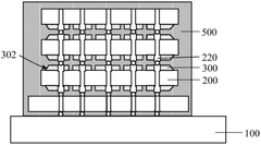
Packaging structure and packaging method
PatentPendingCN120076343A
Innovation
- 采用一种封装结构和方法,其中基板上纵向堆叠的多个芯片的上表面和下表面形成有保护层,导流槽位于保护层中,主导流槽沿模流方向贯穿保护层,支导流槽沿模流方向排布于主导流槽侧部,并向模流方向延伸,形成较大的填充窗口以便塑封料填充。
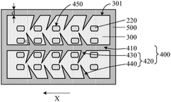

Semiconductor package
PatentPendingUS20250210576A1
Innovation
- A semiconductor package design with multiple stacked semiconductor chip structures and a molding member, utilizing adhesion layers and conductive connection members to enhance electrical connections and prevent warpage, including a TCB and mass reflow process for bonding.


Thermal Management Strategies in HBM4 Design
Thermal management has emerged as a critical factor in the evolution of HBM4 packaging technology, directly impacting both yield and mechanical reliability. As power densities continue to increase with each generation of High Bandwidth Memory, the HBM4 standard introduces several innovative thermal management strategies to address these challenges.
The primary thermal management approach in HBM4 involves advanced materials with superior thermal conductivity properties. Silicon interposers have been redesigned with embedded thermal vias and specialized heat-spreading layers that efficiently channel heat away from critical components. These materials not only improve thermal performance but also maintain dimensional stability under thermal stress, reducing warpage that could compromise mechanical integrity.
Active cooling solutions have been integrated directly into the HBM4 package design. Micro-fluidic cooling channels embedded within the interposer structure allow for targeted heat removal from hotspots, maintaining more uniform temperature distribution across the die stack. This uniformity is crucial for preventing thermally-induced stress that can lead to microcracks and delamination at interface boundaries.
Thermal interface materials (TIMs) between stacked dies have been significantly improved in HBM4 designs. Next-generation TIMs with nanomaterial additives provide up to 45% better thermal conductivity compared to previous generations, while maintaining the mechanical compliance necessary to accommodate coefficient of thermal expansion (CTE) mismatches between different materials in the stack.
Dynamic thermal management systems have been incorporated into HBM4 designs, utilizing embedded temperature sensors and sophisticated power management algorithms. These systems can modulate memory access patterns and power states in response to thermal conditions, preventing thermal runaway scenarios that could compromise reliability while optimizing performance under varying workloads.
Computational fluid dynamics (CFD) modeling has revolutionized the thermal design process for HBM4. Advanced simulation techniques now account for transient thermal behaviors and complex airflow patterns within server environments, enabling more precise thermal management strategies that maintain optimal operating temperatures even under peak load conditions.
The thermal design power (TDP) envelope for HBM4 has been carefully optimized to balance performance requirements with thermal constraints. This optimization extends to the system level, with coordinated thermal management between the HBM4 memory subsystem and adjacent components like GPUs or CPUs, creating a holistic approach to thermal management that significantly improves overall system reliability and performance sustainability.
Supply Chain Considerations for HBM4 Manufacturing
The HBM4 manufacturing ecosystem presents unique supply chain challenges and opportunities that significantly impact yield and mechanical reliability outcomes. The global semiconductor supply chain for advanced packaging technologies like HBM4 requires careful orchestration across multiple tiers of suppliers, with specialized materials and equipment vendors playing critical roles in the overall production process.
Material sourcing represents a fundamental consideration, as HBM4 demands ultra-pure substrates, specialized dielectrics, and advanced metallization materials. The limited number of qualified suppliers for these critical components creates potential bottlenecks that manufacturers must proactively address through strategic partnerships and diversified sourcing strategies. Additionally, the complex nature of HBM4 packaging necessitates specialized equipment for die stacking, TSV formation, and micro-bump bonding, further constraining the supplier ecosystem.
Regional manufacturing capabilities significantly influence HBM4 production strategies. Currently, East Asian countries dominate the advanced packaging landscape, with Taiwan, South Korea, and Japan housing the majority of high-volume manufacturing facilities equipped for HBM4 production. This geographic concentration introduces geopolitical risks that manufacturers must consider when establishing resilient supply chains, potentially driving interest in nearshoring or friendshoring initiatives for critical components.
Inventory management practices directly impact yield outcomes, as the shelf life of certain materials used in HBM4 packaging can affect performance characteristics. Just-in-time manufacturing approaches must be balanced against supply security concerns, particularly for components with extended lead times or limited supplier options. Manufacturers implementing sophisticated inventory tracking systems can optimize material freshness while maintaining production continuity.
Quality control across the supply chain represents another critical factor in HBM4 yield improvement. Implementing standardized testing protocols at multiple points in the supply chain helps identify potential defects before they propagate through the manufacturing process. Advanced suppliers are increasingly adopting digital traceability systems that enable component-level tracking throughout the production lifecycle, facilitating more precise root cause analysis when defects occur.
Collaborative development between HBM4 designers, material suppliers, and equipment manufacturers has emerged as a best practice for addressing supply chain challenges. Early supplier involvement in the design process allows for material and process optimization that can significantly improve both yield and reliability outcomes. These collaborative ecosystems enable faster identification of potential manufacturing constraints and more rapid implementation of corrective measures.
Unlock deeper insights with PatSnap Eureka Quick Research — get a full tech report to explore trends and direct your research. Try now!
Generate Your Research Report Instantly with AI Agent
Supercharge your innovation with PatSnap Eureka AI Agent Platform!