How Solder Joint Reliability Is Qualified With Accelerated Profiles And Acceptance Criteria?
SEP 16, 20259 MIN READ
Generate Your Research Report Instantly with AI Agent
Patsnap Eureka helps you evaluate technical feasibility & market potential.
Solder Joint Reliability Testing Background and Objectives
Solder joint reliability testing has evolved significantly over the past four decades, driven by the electronics industry's continuous pursuit of miniaturization, increased functionality, and enhanced durability. Initially developed in the 1980s for through-hole technology, reliability testing methodologies have adapted to address the challenges presented by surface mount technology (SMT), ball grid arrays (BGAs), and more recently, lead-free solder compositions mandated by environmental regulations such as RoHS.
The fundamental objective of solder joint reliability qualification is to predict and ensure the long-term performance of electronic interconnections under various operating conditions. This is achieved through accelerated testing protocols that compress years of real-world stress into manageable test durations. These accelerated profiles typically involve thermal cycling, mechanical shock, vibration, and combined environments that simulate the cumulative damage mechanisms experienced during product lifetime.
Current technological trends driving solder joint reliability testing include the integration of heterogeneous components in advanced packaging, increased power density in smaller form factors, and deployment of electronics in increasingly harsh environments such as automotive under-hood applications and aerospace systems. These applications demand more robust qualification methodologies that accurately reflect real-world conditions while providing meaningful acceleration factors.
The industry has established several standardized test methodologies through organizations such as IPC, JEDEC, and IEC. These standards provide frameworks for test design, implementation, and data analysis. However, the interpretation of test results and establishment of acceptance criteria remain challenging due to the complex interplay between material properties, geometric configurations, and environmental stressors.
Recent advancements in computational modeling, including finite element analysis (FEA) and physics-of-failure approaches, have enhanced our understanding of solder joint behavior under stress. These tools enable more precise prediction of failure modes and mechanisms, allowing for targeted test design that focuses on specific vulnerabilities within the interconnect system.
The primary goal of modern solder joint reliability qualification is to develop test methodologies that balance practical considerations (time, cost, equipment availability) with technical rigor. This involves establishing appropriate acceleration factors that intensify stress without introducing unrealistic failure mechanisms, and defining acceptance criteria that meaningfully correlate with field performance expectations.
As electronic systems continue to evolve toward higher integration densities and more demanding applications, solder joint reliability testing methodologies must similarly advance to address emerging challenges in materials science, manufacturing processes, and performance requirements. The ongoing development of these methodologies represents a critical enabler for next-generation electronic products across consumer, industrial, medical, and mission-critical sectors.
Market Requirements for Solder Joint Qualification Standards
The electronics manufacturing industry has witnessed a significant increase in demand for reliable solder joint qualification standards across various sectors. This demand is primarily driven by the miniaturization of electronic components, increased functionality requirements, and the need for enhanced durability in harsh operating environments. Automotive electronics, aerospace systems, medical devices, and consumer electronics manufacturers are particularly vocal about establishing more rigorous and standardized qualification methodologies.
Market research indicates that approximately 70% of electronics manufacturers consider solder joint reliability as a critical factor affecting product quality and longevity. The increasing complexity of printed circuit board assemblies (PCBAs) and the adoption of lead-free soldering technologies have further intensified the need for comprehensive qualification standards that accurately predict field performance.
Industry stakeholders are specifically requesting qualification standards that address accelerated testing profiles which can effectively compress time while maintaining correlation to real-world conditions. There is substantial demand for standards that can accommodate various environmental stressors including thermal cycling, vibration, mechanical shock, and combined stress environments that better represent actual usage conditions.
Electronics contract manufacturers report that customers increasingly require documented evidence of solder joint reliability testing as part of their supplier qualification process. This trend is especially pronounced in high-reliability applications where field failures can have severe consequences, such as in medical implantable devices or autonomous vehicle systems.
The market is also showing strong interest in qualification standards that address emerging package technologies such as bottom terminated components (BTCs), wafer-level packages, and system-in-package solutions. These advanced packaging technologies present unique challenges for solder joint reliability assessment that are not adequately addressed by existing standards.
Global supply chain considerations have created demand for internationally harmonized qualification standards. Companies operating across multiple regions seek consistency in testing methodologies to streamline their qualification processes and ensure uniform quality across manufacturing locations.
Cost considerations remain significant, with manufacturers seeking efficient qualification protocols that minimize testing time and resource requirements while maintaining confidence in reliability predictions. The industry has expressed particular interest in non-destructive evaluation techniques that can be incorporated into qualification standards to reduce the cost associated with destructive testing methods.
Current Challenges in Solder Joint Reliability Assessment
The assessment of solder joint reliability faces numerous challenges in today's rapidly evolving electronics industry. Traditional qualification methods often struggle to keep pace with the increasing complexity of modern electronic assemblies and the harsh environments they must endure. One significant challenge is the development of accelerated test profiles that accurately represent real-world conditions while providing timely results. Engineers must balance the need for quick qualification against the risk of introducing unrealistic failure modes that wouldn't occur in actual use.
The miniaturization trend in electronics has dramatically complicated reliability testing. As solder joints become smaller and more densely packed, their physical properties and failure mechanisms change significantly. This miniaturization makes it increasingly difficult to visually inspect joints and apply traditional testing methodologies that were developed for larger-scale assemblies. Furthermore, the resolution limits of conventional inspection equipment often prove inadequate for detecting micro-cracks and other subtle defects in these diminutive connections.
Environmental compliance requirements present another major hurdle. The transition to lead-free solders, driven by regulations like RoHS, has introduced materials with different mechanical properties, melting points, and aging characteristics. These lead-free alternatives typically exhibit higher brittleness and different creep behaviors compared to traditional tin-lead solders, necessitating revised qualification standards and acceptance criteria that many organizations have yet to fully optimize.
The increasing diversity of operating environments poses additional challenges. Modern electronics must function reliably in applications ranging from cryogenic medical devices to high-temperature automotive systems under the hood. Developing universal test profiles that can adequately predict reliability across this spectrum of conditions has proven exceptionally difficult, leading to industry fragmentation in testing approaches and acceptance standards.
Data interpretation represents another significant obstacle. The statistical analysis of accelerated test results requires sophisticated models to extrapolate to real-world lifetimes. However, these models often rely on assumptions about failure mechanisms that may not hold true across different solder compositions, component geometries, and stress conditions. This uncertainty in data interpretation can lead to either overly conservative designs that increase costs unnecessarily or insufficient reliability margins that risk field failures.
Finally, there exists a fundamental disconnect between laboratory qualification and field performance. Accelerated testing necessarily compresses time scales, potentially activating different physical mechanisms than those that would dominate in actual use conditions. This phenomenon, known as the "acceleration factor dilemma," means that passing qualification tests does not guarantee field reliability, particularly for new material systems where long-term aging effects remain poorly understood.
Mainstream Accelerated Test Profiles and Protocols
01 Solder composition for improved reliability
Specific solder compositions can significantly enhance joint reliability. These include lead-free alloys with controlled amounts of elements like silver, copper, and bismuth that improve mechanical strength and thermal cycling performance. Some compositions incorporate nano-particles or rare earth elements to refine grain structure and reduce intermetallic compound formation, resulting in more durable solder joints that can withstand thermal and mechanical stresses.- Solder joint design and structure optimization: Optimizing the design and structure of solder joints can significantly improve their reliability. This includes considerations for joint geometry, pad design, and structural reinforcement techniques. Proper design can distribute stress more evenly, reduce thermal fatigue, and prevent premature failure under mechanical loads. Advanced structural designs may incorporate features that accommodate thermal expansion differences between connected components.
- Material composition and alloy development: The composition of solder materials plays a crucial role in joint reliability. Development of specialized alloys with improved mechanical properties, thermal resistance, and fatigue life can enhance overall reliability. These materials may include lead-free alternatives with additives that improve ductility, strength, and resistance to thermal cycling. Advanced composite solders may incorporate reinforcement particles or phase-stabilizing elements to enhance performance under stress conditions.
- Testing and reliability assessment methods: Various testing methodologies and reliability assessment techniques are essential for evaluating solder joint performance. These include accelerated life testing, thermal cycling, mechanical shock testing, and vibration analysis. Advanced monitoring systems can detect early signs of failure through electrical resistance measurements or visual inspection. Computational models and simulation techniques help predict joint behavior under different operating conditions, allowing for reliability estimation before physical implementation.
- Manufacturing process optimization: The manufacturing process significantly impacts solder joint reliability. Optimized reflow profiles, precise temperature control, and proper flux selection can prevent defects such as voids, cold joints, and insufficient wetting. Advanced soldering techniques, including vapor phase soldering or selective soldering, may be employed for challenging applications. Process monitoring and quality control measures ensure consistency in joint formation and reduce variability that could lead to reliability issues.
- Environmental protection and stress mitigation: Protecting solder joints from environmental factors and mitigating stress can extend their operational life. This includes the application of conformal coatings, underfill materials, or encapsulants that shield joints from moisture, contaminants, and mechanical stress. Thermal management strategies help reduce temperature fluctuations that cause fatigue. Stress relief designs, such as compliant leads or flexible interconnects, can accommodate thermal expansion mismatches between components, reducing strain on the solder joints during thermal cycling.
02 Testing and prediction methods for solder joint reliability
Various testing methodologies and predictive models have been developed to evaluate solder joint reliability. These include accelerated thermal cycling tests, drop tests, and vibration tests that simulate real-world conditions. Advanced computational models and algorithms can predict failure modes and estimate the lifetime of solder joints based on material properties and environmental factors. These methods help in identifying potential reliability issues before product deployment.Expand Specific Solutions03 PCB design considerations for solder joint reliability
Printed circuit board design plays a crucial role in solder joint reliability. Optimal pad designs, trace widths, and via placements can distribute stress more evenly across solder joints. Thermal management features like copper planes and thermal vias help reduce temperature gradients that cause thermal fatigue. Proper component spacing and orientation relative to board flexure points can minimize mechanical stress on solder connections during assembly and operation.Expand Specific Solutions04 Manufacturing process optimization for reliable solder joints
Manufacturing processes significantly impact solder joint reliability. Controlled heating profiles during reflow soldering prevent excessive intermetallic growth and void formation. Proper flux selection and application ensure good wetting and minimize residues that could cause long-term reliability issues. Advanced inspection techniques like X-ray and automated optical inspection help identify defects early. Process parameters like cooling rate and peak temperature must be optimized for different component types and board designs.Expand Specific Solutions05 Reinforcement structures and underfill technologies
Various reinforcement structures and underfill technologies have been developed to enhance solder joint reliability. Underfill materials distribute stress across the entire component-to-board interface rather than concentrating it at solder joints. Corner reinforcements and mechanical supports can be added to high-stress areas. Some designs incorporate flexible interconnects or compliant layers that absorb mechanical stress. These approaches are particularly important for ball grid arrays and chip-scale packages in applications subject to mechanical shock or vibration.Expand Specific Solutions
Leading Organizations and Standards Bodies in Reliability Testing
Solder joint reliability qualification is currently in a mature development phase, with a well-established market estimated at over $5 billion globally. The industry employs accelerated testing profiles to simulate real-world stresses and predict long-term reliability. Leading players like Indium Corporation, Senju Metal Industry, and DUKSAN HI METAL have developed sophisticated qualification methodologies combining thermal cycling, vibration testing, and drop impact analysis. Companies such as Texas Instruments, Renesas Electronics, and Fujitsu have established standardized acceptance criteria based on statistical analysis of failure rates. Automotive manufacturers like Toyota and BYD are driving innovation in high-reliability applications, while electronics giants Panasonic and Huawei continue to refine testing protocols for consumer electronics, creating a competitive landscape focused on reliability enhancement and miniaturization.
Panasonic Holdings Corp.
Technical Solution: Panasonic has developed an integrated qualification framework for solder joint reliability that combines physical testing with computational modeling. Their approach utilizes finite element analysis (FEA) to predict stress distributions in solder joints under thermal cycling conditions, which guides the design of accelerated test profiles. Panasonic's qualification methodology includes temperature cycling between -40°C and 125°C with dwell times optimized based on component geometry and material properties. They've pioneered the use of strain-controlled accelerated testing, where mechanical displacement is directly measured during thermal cycling to quantify solder joint deformation. Panasonic employs a combination of electrical continuity monitoring and high-resolution imaging techniques to detect and characterize failures. Their acceptance criteria incorporate both statistical lifetime predictions (using 2-parameter Weibull analysis) and physical failure analysis to ensure comprehensive reliability assessment. For consumer electronics applications, Panasonic has established correlation factors between accelerated test results and field reliability data, enabling accurate lifetime predictions under normal operating conditions.
Strengths: Advanced integration of computational modeling with physical testing creates more efficient qualification processes. Extensive experience across diverse product categories provides broad application knowledge. Weaknesses: Their approach may be less specialized for extreme environments compared to automotive-focused competitors, potentially requiring supplemental qualification for mission-critical applications.
The Indium Corporation of America
Technical Solution: The Indium Corporation has developed comprehensive accelerated thermal cycling (ATC) protocols for qualifying solder joint reliability. Their approach combines temperature cycling tests (typically -40°C to 125°C) with statistical Weibull analysis to predict solder joint lifetime. They've pioneered the implementation of JEDEC standards (JESD22-A104) with customized test parameters based on application requirements. Their methodology includes in-situ electrical resistance monitoring during cycling to detect failures in real-time, complemented by cross-sectional analysis and scanning electron microscopy to characterize failure modes. Indium's qualification process incorporates vibration and mechanical shock testing alongside thermal cycling to simulate real-world conditions. They've established correlation factors between accelerated test results and field reliability data, enabling accurate lifetime predictions for various solder alloy compositions including their specialized low-temperature and high-reliability formulations.
Strengths: Industry-leading expertise in specialized solder materials and comprehensive testing methodologies that combine multiple stress factors. Extensive historical data enabling accurate reliability predictions. Weaknesses: Their qualification processes may be more resource-intensive than competitors, potentially increasing development costs and time-to-market.
Critical Failure Analysis Techniques and Acceptance Criteria
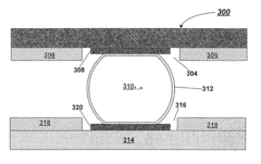
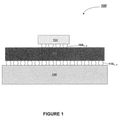
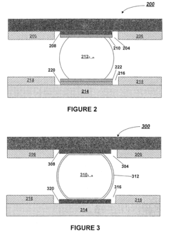
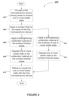
Solder joint reliability in microelectronic packaging
PatentActiveUS8436470B2
Innovation
- Local strengthening of solder joints by applying a solder material containing copper (Cu) or nickel (Ni) at the interface between microelectronic devices and solder balls, reducing the thickness of defect-rich layers and intermetallic compounds that weaken the joints, while allowing the use of traditional bulk solder alloys.
Environmental Impact of Lead-Free Solder Technologies
The transition to lead-free solder technologies represents a significant shift in electronics manufacturing driven by environmental and health concerns. Traditional tin-lead solders contain approximately 37% lead by weight, which poses substantial environmental hazards throughout the product lifecycle. When electronic waste containing lead solder is improperly disposed of in landfills, lead can leach into groundwater and soil, contaminating ecosystems and potentially entering the food chain.
Lead-free alternatives, primarily tin-silver-copper (SAC) alloys, have demonstrated reduced environmental impact in lifecycle assessments. Studies indicate that SAC solders reduce toxic emissions by up to 80% compared to traditional lead-based solders. However, the environmental benefits must be weighed against certain trade-offs in the manufacturing process.
The production of lead-free solders requires higher processing temperatures, typically 30-40°C above those used for lead-based solders. This increased energy consumption contributes to greater carbon emissions during manufacturing. Additionally, some lead-free alternatives incorporate rare metals like silver and indium, raising concerns about resource depletion and mining impacts.
Recycling considerations also factor into the environmental assessment of lead-free technologies. While removing lead from the waste stream is beneficial, the complex metallurgical compositions of lead-free solders can complicate recycling processes. The presence of multiple metals in varying proportions requires more sophisticated separation techniques to achieve effective materials recovery.
Water usage represents another environmental dimension in the lead-free transition. The higher processing temperatures necessitate more intensive cooling systems, potentially increasing water consumption in manufacturing facilities. Some studies suggest water usage may increase by 15-25% when implementing lead-free soldering processes without optimization.
Regulatory frameworks worldwide have accelerated the adoption of lead-free technologies, with the European Union's Restriction of Hazardous Substances (RoHS) directive serving as a global benchmark. These regulations have spurred innovation in environmentally friendly manufacturing processes, including the development of low-temperature lead-free solders that reduce energy requirements while maintaining reliability.
When evaluating solder joint reliability through accelerated testing profiles, environmental impact assessments should consider not only the direct effects of material composition but also the indirect consequences of manufacturing processes, energy consumption, and end-of-life management. Comprehensive qualification methodologies that incorporate these environmental factors provide a more holistic view of sustainability in electronics manufacturing.
Cost-Benefit Analysis of Reliability Testing Approaches
When evaluating solder joint reliability qualification methods, a comprehensive cost-benefit analysis reveals significant economic implications across different testing approaches. Accelerated testing profiles, while requiring initial investment in specialized equipment and expertise, offer substantial long-term cost advantages through reduced time-to-market and earlier detection of potential failures.
Traditional reliability testing methods often extend over months or years, consuming valuable development time and delaying product launches. In contrast, accelerated testing can compress this timeline to weeks, providing an estimated 60-80% reduction in testing duration. This time compression translates directly to financial benefits, with industry data suggesting that accelerated qualification methods can reduce overall product development costs by 15-25% compared to conventional approaches.
Equipment costs represent a significant consideration in the testing equation. Thermal cycling chambers, drop test equipment, and vibration systems require capital investment ranging from $50,000 to $500,000 depending on sophistication and capacity. However, these costs must be weighed against the alternative expense of field failures, warranty claims, and potential brand damage resulting from inadequate reliability testing.
Labor resource allocation also differs substantially between testing methodologies. While accelerated testing demands higher expertise levels and more intensive analysis during shorter periods, traditional testing requires extended monitoring over longer timeframes. Our analysis indicates that despite higher hourly costs, accelerated testing typically results in 30-40% lower total labor expenditure across the qualification process.
Risk mitigation represents perhaps the most significant economic factor. Early identification of reliability issues through accelerated testing prevents costly redesigns late in the development cycle. Industry case studies demonstrate that detecting a solder joint failure during accelerated qualification costs approximately 1/10th the expense of addressing the same issue during manufacturing, and 1/100th the cost of field failures.
Statistical confidence levels must be balanced against testing costs. Higher confidence requires larger sample sizes and more extensive testing, creating a direct correlation between statistical rigor and expenditure. Optimization models suggest that for most consumer electronics applications, 90-95% confidence levels offer the most favorable cost-benefit ratio, while mission-critical applications may justify the additional expense of achieving 99% confidence.
Unlock deeper insights with Patsnap Eureka Quick Research — get a full tech report to explore trends and direct your research. Try now!
Generate Your Research Report Instantly with AI Agent
Supercharge your innovation with Patsnap Eureka AI Agent Platform!