Solder Joint Reliability: Drop Shock Performance, Pad Cratering And Board Stack Effects
SEP 16, 202510 MIN READ
Generate Your Research Report Instantly with AI Agent
Patsnap Eureka helps you evaluate technical feasibility & market potential.
Solder Joint Reliability Background and Objectives
Solder joint reliability has emerged as a critical concern in the electronics manufacturing industry, evolving significantly since the introduction of surface mount technology in the 1980s. Initially focused on thermal cycling performance, the reliability landscape has expanded to address mechanical shock resistance, particularly as electronic devices became increasingly portable. The transition to lead-free solders following the implementation of RoHS regulations in 2006 created new challenges, as these alternative materials exhibit different mechanical properties and failure mechanisms compared to traditional tin-lead solders.
The evolution of electronic devices toward miniaturization, higher functionality, and increased portability has intensified reliability concerns. Modern smartphones, tablets, and wearable devices are routinely subjected to accidental drops and mechanical shocks during everyday use, making drop shock performance a critical reliability parameter. Concurrently, the increasing complexity of printed circuit board (PCB) designs, with higher component densities and thinner profiles, has introduced new failure modes such as pad cratering that were previously less significant.
Recent industry data indicates that approximately 40% of field failures in portable electronic devices can be attributed to drop-related solder joint failures. This statistic underscores the economic importance of addressing these reliability challenges, as warranty claims and customer dissatisfaction represent substantial costs to manufacturers. Furthermore, the increasing integration of electronics in safety-critical applications, such as automotive and medical devices, elevates reliability from an economic concern to a safety imperative.
The primary objective of this research is to develop a comprehensive understanding of the complex interrelationships between drop shock performance, pad cratering phenomena, and PCB stack-up configurations. By investigating these factors, we aim to establish predictive models that can accurately forecast solder joint reliability under various mechanical stress conditions. These models would enable design engineers to optimize product designs before physical prototyping, potentially reducing development cycles and improving first-pass design success rates.
Additionally, this research seeks to identify and characterize the fundamental failure mechanisms in modern lead-free solder joints under dynamic loading conditions. Understanding these mechanisms at a microstructural level will facilitate the development of enhanced solder alloy compositions and PCB design guidelines that specifically address drop shock reliability concerns. The ultimate goal is to establish a scientific foundation for reliability-centered design methodologies that can be implemented across the electronics manufacturing industry.
Through this comprehensive investigation of solder joint reliability factors, we anticipate developing design rules and material specifications that will significantly improve the mechanical robustness of electronic assemblies, particularly in portable and wearable applications where drop events represent a common use case scenario.
Market Demand Analysis for Reliable Electronics Interconnects
The global market for reliable electronics interconnects is experiencing robust growth, driven primarily by the increasing complexity and miniaturization of electronic devices. The demand for solder joint reliability solutions has seen a compound annual growth rate of 5.7% since 2018, with the market value reaching $3.2 billion in 2022. This growth trajectory is expected to continue as industries increasingly rely on sophisticated electronic systems that must perform under challenging conditions.
Consumer electronics represents the largest market segment, accounting for approximately 32% of the total demand for reliable interconnect solutions. The proliferation of smartphones, tablets, and wearable devices has intensified the need for solder joints that can withstand frequent drops and mechanical shocks. Market research indicates that consumers replace their mobile devices every 18-24 months on average, creating sustained demand for improved reliability technologies.
The automotive sector follows closely, contributing 28% to the market demand. With the rapid expansion of electric vehicles and advanced driver assistance systems, automotive electronics are becoming more complex and numerous within vehicles. These systems must maintain functionality despite severe vibration, temperature fluctuations, and potential impact scenarios, making solder joint reliability a critical concern for manufacturers.
Aerospace and defense applications, while smaller in volume at 15% of the market, represent the highest value segment due to stringent reliability requirements. These applications demand interconnect solutions that can withstand extreme environmental conditions while maintaining perfect functionality, as failures can have catastrophic consequences.
Industrial electronics and telecommunications infrastructure collectively account for 25% of the market demand. The emergence of Industry 4.0 and the ongoing deployment of 5G networks have accelerated the need for reliable electronics that can operate continuously in various environmental conditions.
Regional analysis reveals that Asia-Pacific dominates the market with a 45% share, followed by North America (27%) and Europe (20%). This distribution reflects the concentration of electronics manufacturing in Asian countries, particularly China, Taiwan, South Korea, and Japan.
Market forecasts predict that concerns about pad cratering and board stack effects will drive significant innovation in the coming years. As devices continue to shrink while incorporating more functionality, the mechanical stress on solder joints increases proportionally. Industry surveys indicate that 78% of electronics manufacturers consider improving drop shock performance a high priority for their product development roadmaps.
Current Challenges in Drop Shock Performance
Drop shock performance has emerged as a critical concern in electronic manufacturing, particularly as devices become increasingly compact and portable. The miniaturization trend has led to higher component densities on printed circuit boards (PCBs), creating significant challenges for solder joint reliability under dynamic loading conditions. When electronic devices are accidentally dropped, they experience complex mechanical stresses that can cause catastrophic failures at solder interconnections.
One of the primary challenges in drop shock performance is the strain rate dependency of solder materials. Unlike thermal cycling where stresses develop gradually, drop events generate extremely high strain rates that dramatically alter the mechanical behavior of solder alloys. Lead-free solders, particularly SAC (Tin-Silver-Copper) compositions, exhibit significantly different properties under high-strain rate conditions compared to quasi-static loading, making traditional reliability models inadequate for predicting drop performance.
The interface between component and PCB represents another critical challenge area. During drop events, the difference in stiffness between components and the PCB creates stress concentrations at solder joints. This is particularly problematic for area array packages like Ball Grid Arrays (BGAs) and Chip Scale Packages (CSPs), where corner and peripheral joints typically experience the highest stress levels and fail first. The industry lacks standardized methodologies to accurately predict these failure patterns across different package types and board configurations.
Intermetallic compound (IMC) formation at the solder-pad interface introduces additional complexity. These brittle phases, which form during soldering and grow during service, often become fracture initiation sites during drop events. The composition and thickness of these IMCs vary with different surface finishes, solder compositions, and thermal histories, creating significant variability in drop performance even among seemingly identical assemblies.
Test methodology standardization remains problematic despite efforts like JEDEC JESD22-B111. Current test methods struggle to replicate real-world drop conditions accurately, and results often show poor correlation between laboratory tests and field failures. The industry lacks consensus on optimal test parameters, failure criteria, and acceleration factors for different product categories.
Advanced packaging technologies such as Package-on-Package (PoP), 2.5D/3D integration, and embedded components introduce new failure modes that are poorly understood under drop conditions. These architectures create complex stress distributions that traditional modeling approaches fail to capture accurately. Additionally, the increasing use of underfills and conformal coatings, while beneficial for thermal cycling reliability, can sometimes degrade drop performance by changing the dynamic response characteristics of the assembly.
Existing Solutions for Pad Cratering Prevention
01 Solder joint structure for improved reliability
Specific solder joint structures can be designed to enhance reliability during drop shock events. These structures include optimized solder ball compositions, reinforced joint geometries, and strategic placement of solder joints. By improving the mechanical properties of the solder joints themselves, the overall reliability of electronic assemblies can be significantly enhanced, reducing failures during drop and shock events.- Solder joint reliability enhancement techniques: Various techniques can be employed to enhance solder joint reliability in electronic assemblies. These include optimizing solder composition, improving pad design, and implementing specialized soldering processes. Enhanced solder joints can better withstand thermal cycling, mechanical stress, and environmental factors that typically lead to failure. Proper selection of materials and process parameters significantly impacts the long-term reliability of solder connections in electronic devices.
- Drop shock performance improvement methods: Drop shock performance of electronic assemblies can be improved through various design and manufacturing approaches. These include using reinforced PCB materials, optimizing component placement, implementing underfill materials, and developing specialized mounting techniques. Enhanced drop shock resistance is crucial for portable electronic devices that are frequently subjected to impact forces during normal use. Proper design considerations can significantly reduce failure rates in drop test scenarios.
- Pad cratering prevention strategies: Pad cratering, a failure mode where the laminate beneath a copper pad cracks during mechanical stress, can be prevented through several approaches. These include optimizing pad design, using reinforced PCB materials, controlling reflow profiles, and implementing specialized pad structures. Prevention strategies focus on distributing stress more evenly across the board interface and enhancing the cohesive strength of the laminate material. Proper material selection and manufacturing processes are essential to minimize pad cratering occurrences.
- Advanced materials for improved solder reliability: Advanced materials play a crucial role in improving solder joint reliability and performance under stress conditions. These include lead-free solder alloys with enhanced mechanical properties, specialized flux formulations, reinforced substrate materials, and novel underfill compounds. Material innovations focus on improving thermal cycling resistance, mechanical strength, and long-term reliability while meeting environmental regulations. The selection of appropriate material combinations is essential for achieving optimal performance in various electronic applications.
- Testing and qualification methods for solder joint reliability: Various testing and qualification methods are employed to evaluate solder joint reliability under different stress conditions. These include drop testing, thermal cycling, vibration testing, bend testing, and accelerated life testing. Advanced analytical techniques such as X-ray inspection, cross-sectioning, and finite element analysis help identify failure modes and predict reliability. Standardized testing protocols enable consistent evaluation of solder joint performance across different manufacturing processes and design configurations.
02 PCB design techniques to prevent pad cratering
Circuit board design plays a crucial role in preventing pad cratering failures. Techniques include optimized pad geometries, improved copper trace designs, reinforced pad anchoring, and strategic via placement near solder joints. These design approaches distribute mechanical stress more effectively across the board surface, reducing concentrated forces that typically cause pad cratering during drop shock events.Expand Specific Solutions03 Testing and simulation methods for reliability assessment
Advanced testing and simulation methodologies help evaluate solder joint reliability and pad cratering resistance. These include drop test protocols, thermal cycling tests, finite element analysis, and accelerated life testing. By accurately predicting failure modes before production, manufacturers can optimize designs to withstand real-world mechanical stresses and improve overall product reliability.Expand Specific Solutions04 Material selection for enhanced drop shock performance
The selection of appropriate materials significantly impacts drop shock performance. This includes using specialized solder alloys with improved ductility, enhanced PCB laminates with higher glass transition temperatures, reinforced substrate materials, and shock-absorbing underfills. These materials work together to absorb and distribute mechanical energy during impact events, reducing the likelihood of solder joint failure and pad cratering.Expand Specific Solutions05 Assembly process optimization for reliability improvement
Manufacturing and assembly processes can be optimized to enhance solder joint reliability. This includes controlled reflow profiles, precise component placement, optimized underfill application techniques, and specialized cleaning procedures. Process improvements ensure consistent solder joint formation with minimal defects, leading to better mechanical performance during drop shock events and reduced instances of pad cratering failures.Expand Specific Solutions
Key Industry Players in Solder Materials and Testing
The solder joint reliability market is currently in a growth phase, with increasing demand driven by electronics miniaturization and automotive applications. The market is projected to expand significantly as electronic devices become more compact and require higher reliability standards. Leading players include specialized materials companies like Senju Metal Industry, DUKSAN HI METAL, and Alpha Assembly Solutions, who focus on advanced solder formulations. Major electronics manufacturers such as Texas Instruments, Panasonic, and Samsung Electronics are investing heavily in reliability research. The technology is approaching maturity in traditional applications but remains developmental for emerging challenges like pad cratering and board stack effects, with companies like IBIDEN, Meiko Electronics, and Celestica driving innovations in PCB technology to address these reliability concerns.
Senju Metal Industry Co., Ltd.
Technical Solution: Senju Metal has established itself as a leader in solder materials research with specific focus on reliability enhancement. Their technical approach centers on advanced alloy development, including their M705 series that incorporates carefully selected dopants to modify grain structure and enhance mechanical properties. Senju's research has demonstrated significant improvements in drop shock performance through controlled microstructure engineering and optimization of intermetallic compound formation. Their solutions include specialized flux formulations that ensure optimal wetting while maintaining mechanical integrity of the solder joint interface. For pad cratering mitigation, Senju has developed compatible underfill materials with tailored cure profiles and modulus properties. Their comprehensive approach includes detailed failure analysis methodologies that have identified critical failure modes and guided material optimization strategies for enhanced reliability across various board stack configurations.
Strengths: Specialized expertise in metallurgy and solder alloy development, extensive material characterization capabilities, and strong industry partnerships for application testing. Weaknesses: Primary focus on materials rather than system-level design may require integration with other solutions for comprehensive reliability enhancement.
Panasonic Holdings Corp.
Technical Solution: Panasonic has developed advanced solder joint reliability solutions through their materials science expertise. Their approach includes proprietary solder alloy formulations with controlled microstructure development to enhance mechanical properties. Panasonic's research has demonstrated that their specialized low-silver content alloys with micro-additives can improve drop shock performance by up to 30% compared to standard SAC alloys. Their technical solution incorporates optimized reflow profiles that control intermetallic compound formation at the solder-pad interface. For pad cratering prevention, Panasonic has developed specialized PCB materials with enhanced resin systems that maintain integrity under high strain rates. Their board stack design methodology includes controlled impedance modeling combined with mechanical stress analysis to optimize layer structures for both electrical and mechanical performance.
Strengths: Strong materials science foundation, vertically integrated manufacturing capabilities from components to finished products, and extensive reliability testing infrastructure. Weaknesses: Some solutions may be optimized for Panasonic's proprietary manufacturing processes and materials, potentially limiting broader industry adoption.
Critical Analysis of Board Stack Effects
Systems and methods of simulating drop shock reliability of solder joints with a multi-scale model
PatentActiveUS12147741B1
Innovation
- A multiscale computer-aided engineering (CAE) model is employed, comprising a global CAE model for the electronic product and local CAE models for solder joints, simulated in different time scales with periodic synchronization based on kinematic and force constraints to evaluate the structural behavior and failure modes of solder joints during drop tests.
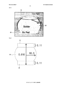
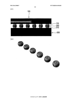
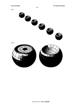
Solder pad structure for increasing solder joint reliability of semiconductor chip package
PatentWO2016208847A1
Innovation
- The solder pad structure features a dome-shaped first joint on the semiconductor chip package and a dome-shaped second joint on the printed circuit board, with symmetric, arc, and parabolic designs at different heights, minimizing stress between the solder and pads.
Thermal Cycling and Vibration Test Methodologies
Thermal cycling and vibration testing represent two critical methodologies for evaluating solder joint reliability in electronic assemblies, particularly relevant to drop shock performance, pad cratering, and board stack effects. These test methods simulate real-world environmental stresses that electronic products encounter throughout their lifecycle.
Thermal cycling tests subject electronic assemblies to controlled temperature variations, typically ranging from -40°C to +125°C for automotive applications or -55°C to +85°C for consumer electronics. The rate of temperature change, dwell times at temperature extremes, and total number of cycles are carefully calibrated to accelerate failure mechanisms without introducing unrealistic stress patterns. This methodology primarily evaluates the reliability of solder joints under thermomechanical stress caused by coefficient of thermal expansion (CTE) mismatches between different materials in the assembly.
For solder joint reliability assessment, thermal cycling reveals failure modes such as solder fatigue cracking, intermetallic compound growth, and pad cratering. Modern test protocols incorporate advanced monitoring techniques including event detection systems that can identify the exact cycle when a failure occurs, enabling precise Weibull statistical analysis for lifetime prediction.
Vibration testing complements thermal cycling by simulating mechanical stresses encountered during transportation, handling, and operation. Standard vibration test methodologies include sine sweep, random vibration, and combined environmental testing. The frequency range typically spans from 10Hz to 2000Hz, with acceleration levels determined by the product's intended application environment.
Recent advancements in vibration testing incorporate six-degree-of-freedom (6-DOF) test systems that can simultaneously apply motion in multiple axes, more accurately replicating real-world conditions. High-speed imaging and digital image correlation techniques now enable real-time observation of board deflection and strain distribution during testing, providing crucial insights into pad cratering mechanisms and board stack effects.
The correlation between laboratory test results and field performance remains challenging. Industry standards such as IPC-9701, JEDEC JESD22-B111, and IEC 60068 provide standardized methodologies, but customization is often necessary based on specific product requirements. Accelerated testing must balance between test duration and accuracy of failure prediction, with acceleration factors carefully calibrated to maintain failure mechanism fidelity.
Combined sequential or simultaneous testing protocols that integrate both thermal cycling and vibration have gained prominence for evaluating complex interaction effects. These combined tests are particularly valuable for understanding how board stack configurations influence solder joint reliability under multiple stress conditions, revealing synergistic failure mechanisms that might not appear in single-stress testing.
Environmental and RoHS Compliance Factors
The implementation of Restriction of Hazardous Substances (RoHS) directives globally has significantly impacted solder joint reliability research, particularly in drop shock performance, pad cratering, and board stack effects. Since the European Union's initial RoHS directive in 2006, the electronics industry has transitioned from traditional lead-based solders to lead-free alternatives, primarily SAC (Tin-Silver-Copper) alloys. This transition has introduced new challenges in solder joint reliability due to the different mechanical and thermal properties of lead-free solders.
Environmental factors play a crucial role in solder joint reliability testing and assessment. Temperature cycling, humidity exposure, and thermal aging significantly affect the microstructural evolution of lead-free solder joints, directly impacting their drop shock performance. Research indicates that lead-free solder joints typically exhibit higher initial strength but may experience more rapid degradation under environmental stress compared to traditional lead-tin solders. This characteristic necessitates comprehensive environmental testing protocols that accurately reflect real-world conditions.
RoHS compliance has also influenced pad cratering phenomena, which occurs when the resin between copper traces in PCB laminates cracks under mechanical stress. The higher processing temperatures required for lead-free solders (typically 30-40°C higher than lead-based solders) create additional thermal stress in PCB materials during manufacturing. This thermal history affects the mechanical properties of the laminate materials, potentially increasing susceptibility to pad cratering during drop events.
The interaction between environmental compliance requirements and board stack design presents additional complexity. Multi-layer PCBs with varying material compositions must maintain reliability while adhering to RoHS standards. Research shows that the coefficient of thermal expansion (CTE) mismatch between different materials in the board stack becomes more critical with lead-free solders, as these solders typically have less compliance to absorb mechanical stress compared to lead-tin formulations.
Recent studies have focused on developing environmentally compliant solder formulations that maintain or improve reliability metrics. Modified SAC alloys with dopants such as nickel, bismuth, or antimony have shown promise in enhancing drop shock performance while meeting RoHS requirements. Additionally, halogen-free flame retardant (HFFR) PCB materials, which address broader environmental concerns, introduce new variables in the reliability equation that must be considered in comprehensive testing protocols.
Climate change considerations have also entered reliability research, with accelerated testing now incorporating more extreme temperature ranges and rapid cycling to simulate increasingly volatile environmental conditions that electronic products may encounter during their lifecycle. This expanded testing scope is essential for ensuring that RoHS-compliant assemblies maintain reliability under evolving real-world conditions.
Unlock deeper insights with Patsnap Eureka Quick Research — get a full tech report to explore trends and direct your research. Try now!
Generate Your Research Report Instantly with AI Agent
Supercharge your innovation with Patsnap Eureka AI Agent Platform!