Solder Joint Reliability: Reflow Profiles, IMC Thickness Control And Residual Flux Effects
SEP 16, 20259 MIN READ
Generate Your Research Report Instantly with AI Agent
Patsnap Eureka helps you evaluate technical feasibility & market potential.
Solder Joint Reliability Background and Objectives
Solder joint reliability has emerged as a critical concern in the electronics manufacturing industry since the 1970s, evolving significantly with the transition from through-hole technology to surface mount technology (SMT). This evolution has been further accelerated by the global shift toward lead-free soldering processes following environmental regulations such as the European Union's Restriction of Hazardous Substances (RoHS) directive implemented in 2006. The reliability challenges have intensified as electronic devices continue to miniaturize while simultaneously requiring higher performance and longer operational lifespans.
The historical development of solder joint technology reveals a progressive understanding of failure mechanisms. Early research focused primarily on mechanical failures, but as computational capabilities advanced, more sophisticated models incorporating thermal cycling, vibration effects, and electrochemical migration emerged. The industry has witnessed a paradigm shift from reactive failure analysis to proactive reliability engineering, emphasizing prevention rather than remediation.
Current technological trends indicate growing complexity in solder joint reliability factors. The increasing density of components on printed circuit boards (PCBs), the proliferation of flexible and rigid-flex substrates, and the adoption of heterogeneous integration all contribute to new reliability challenges. Additionally, the automotive and aerospace sectors are driving demands for extreme reliability under harsh environmental conditions, pushing conventional soldering technologies to their limits.
The intermetallic compound (IMC) layer formed during the soldering process represents a double-edged sword for reliability. While necessary for establishing electrical and mechanical connections, excessive IMC growth often leads to brittle interfaces prone to failure under thermal or mechanical stress. Controlling IMC thickness has therefore become a central focus in reliability engineering, with significant research dedicated to understanding the relationship between reflow profiles and IMC formation kinetics.
Residual flux effects constitute another critical dimension of reliability concerns. Modern no-clean flux formulations, while offering manufacturing advantages, can leave residues that potentially compromise long-term reliability through electrochemical migration or dendritic growth. The interaction between these residues and environmental factors such as humidity and contamination presents ongoing challenges for reliability prediction and testing methodologies.
The primary objectives of current research in solder joint reliability include developing comprehensive models that accurately predict reliability across diverse operating conditions, establishing standardized testing protocols that correlate with real-world performance, and formulating advanced materials and processes that enhance reliability while meeting environmental regulations. Additionally, there is growing interest in creating design guidelines that incorporate reliability considerations from the earliest stages of product development, rather than addressing them as afterthoughts.
Market Demand Analysis for High-Reliability Soldering
The global market for high-reliability soldering solutions is experiencing robust growth driven by increasing demands across multiple industries. The electronics manufacturing sector, particularly in aerospace, defense, medical devices, and automotive applications, requires soldering technologies that can withstand extreme conditions while maintaining long-term operational integrity. Current market estimates value the high-reliability soldering segment at approximately $3.5 billion, with projected annual growth rates of 6-8% through 2028.
Consumer electronics continues to be the largest market segment, accounting for nearly 40% of demand. However, the fastest growth is observed in automotive electronics, particularly with the rapid expansion of electric vehicles (EVs) and advanced driver-assistance systems (ADAS). These applications require solder joints capable of withstanding thermal cycling, vibration, and mechanical stress while maintaining electrical conductivity over extended periods.
The medical device industry represents another significant growth area, where device miniaturization and implantable technologies demand exceptionally reliable solder connections. Failure in these applications can have life-threatening consequences, driving stringent requirements for solder joint reliability and creating premium market opportunities for advanced soldering solutions.
Geographically, Asia-Pacific dominates manufacturing volume, but North America and Europe lead in high-reliability applications and technological innovation. China's manufacturing sector is rapidly advancing in this space, investing heavily in reliability improvements to capture higher-value segments of the electronics manufacturing market.
Market research indicates that customers are increasingly focused on three key aspects of soldering reliability: optimized reflow profiles that minimize thermal stress, controlled intermetallic compound (IMC) thickness for balanced strength and ductility, and effective management of residual flux to prevent long-term corrosion and electrical failures. These technical factors directly impact product longevity, warranty costs, and brand reputation.
The market is also witnessing a shift toward lead-free soldering technologies that maintain or exceed the reliability of traditional lead-based solders while meeting environmental regulations. This transition has created significant demand for research into alternative alloy compositions and process optimizations that can deliver comparable or superior performance characteristics.
Industry surveys reveal that manufacturers are willing to pay premium prices for soldering technologies that demonstrably improve reliability metrics, particularly mean-time-between-failures (MTBF) and thermal cycling resistance. This price elasticity creates substantial opportunities for innovative solutions that address the specific challenges of IMC formation control and flux residue management.
Current Challenges in Solder Joint Technology
The solder joint reliability landscape faces significant challenges as electronic devices continue to miniaturize while demanding higher performance and durability. Current manufacturing processes struggle with inconsistent reflow profiles, which directly impact the formation and quality of solder joints. Temperature gradients across printed circuit boards (PCBs) create non-uniform heating, resulting in varying degrees of solder melting and solidification that compromise joint integrity. This variability becomes particularly problematic in complex assemblies with components of different thermal masses.
Intermetallic compound (IMC) thickness control represents another critical challenge. While IMCs are essential for establishing mechanical bonds between solder and substrate, excessive IMC growth—particularly during thermal cycling—leads to brittle interfaces prone to fracture. The industry lacks standardized methods to precisely control IMC formation during manufacturing and limit its continued growth during service life. This challenge is exacerbated by the transition to lead-free solders, which typically form thicker and more complex IMC layers compared to traditional tin-lead compositions.
Residual flux effects constitute a persistent reliability concern that has gained prominence with increased circuit density. Modern electronic assemblies leave minimal clearance between components and substrates, creating areas where flux residues become trapped after the soldering process. These residues, if not properly removed or neutralized, can cause electrochemical migration, leading to current leakage and eventual short circuits. The corrosive nature of certain flux chemistries further accelerates degradation of metallic elements within the assembly.
Environmental factors compound these technical challenges. The electronics industry faces increasing pressure to withstand harsh operating conditions while extending product lifespans. Thermal cycling, humidity, vibration, and mechanical shock all accelerate the deterioration of solder joints affected by the aforementioned issues. The automotive and aerospace sectors, in particular, demand solder connections that maintain integrity across extreme temperature ranges and high-vibration environments.
Manufacturing scalability presents additional complications. Techniques that might address these challenges in laboratory settings often prove difficult to implement in high-volume production environments. The cost-performance balance remains delicate, with manufacturers reluctant to adopt solutions that significantly increase production costs or cycle times, even when reliability improvements are demonstrable. This economic constraint limits the practical application of certain advanced materials and processes that could otherwise enhance solder joint performance.
Current Methodologies for IMC Thickness Control
01 Solder composition and material selection
The reliability of solder joints is significantly influenced by the composition of solder materials used. Various alloy compositions can enhance mechanical strength, thermal cycling resistance, and overall durability of the joints. Advanced materials such as lead-free solders with specific additives can improve performance under thermal stress and prevent common failure modes. The selection of appropriate solder materials based on application requirements is crucial for ensuring long-term reliability in electronic assemblies.- Solder composition and material selection: The reliability of solder joints is significantly influenced by the composition of solder materials used. Various alloy compositions can enhance mechanical strength, thermal cycling resistance, and overall durability of the joints. Advanced materials such as lead-free solders with specific additives can improve crack resistance and extend the operational lifespan of electronic connections. The selection of appropriate solder materials based on application requirements is crucial for ensuring long-term reliability under various environmental conditions.
- Thermal cycling and stress management: Solder joint reliability is heavily dependent on how well the joints can withstand thermal cycling and mechanical stress. Temperature fluctuations cause expansion and contraction that can lead to fatigue failure. Implementing proper stress management techniques, such as using underfill materials, optimizing pad designs, and incorporating stress-relief features in PCB layouts can significantly improve joint durability. Testing under accelerated thermal cycling conditions helps predict long-term reliability and identify potential failure modes before deployment.
- Manufacturing process optimization: The manufacturing process significantly impacts solder joint reliability. Factors such as reflow profile, cooling rate, and soldering environment must be carefully controlled to achieve optimal joint formation. Advanced techniques like vacuum soldering, controlled atmosphere soldering, and precise temperature profiling can reduce void formation and improve intermetallic compound structures. Process monitoring and quality control measures during manufacturing ensure consistency and reliability across production batches.
- Testing and reliability prediction methods: Various testing methodologies and reliability prediction techniques are essential for evaluating solder joint performance. These include accelerated life testing, thermal shock testing, vibration analysis, and advanced imaging techniques such as X-ray inspection and acoustic microscopy. Computational models and simulation tools can predict failure mechanisms and estimate the lifetime of solder joints under different operating conditions. Real-time monitoring systems can detect early signs of joint degradation, allowing for preventive maintenance before catastrophic failure occurs.
- PCB design and pad configuration: The design of printed circuit boards and pad configurations significantly affects solder joint reliability. Optimized pad geometries, appropriate surface finishes, and strategic component placement can reduce stress concentration and improve joint strength. Design considerations such as thermal management features, proper spacing between components, and the use of via-in-pad technology can enhance the overall reliability of solder connections. Advanced PCB materials with matched coefficients of thermal expansion can minimize stress during temperature fluctuations.
02 Thermal cycling and stress management
Thermal cycling is a major factor affecting solder joint reliability. Methods to manage thermal stress include optimized joint geometry, stress relief designs, and thermal management techniques. Controlling coefficient of thermal expansion (CTE) mismatches between components and substrates helps prevent fatigue failures. Implementing proper thermal profiles during soldering processes and in operational environments can significantly extend the lifespan of solder connections and reduce failure rates in electronic assemblies.Expand Specific Solutions03 Testing and reliability prediction methods
Advanced testing methodologies are essential for predicting and ensuring solder joint reliability. These include accelerated life testing, thermal shock testing, vibration analysis, and non-destructive inspection techniques. Computational models and simulation tools help predict failure mechanisms and optimize joint designs before physical implementation. Real-time monitoring systems can detect early signs of joint degradation, allowing for preventive maintenance and improved reliability assessment throughout the product lifecycle.Expand Specific Solutions04 Manufacturing process optimization
The manufacturing process significantly impacts solder joint reliability. Optimized reflow profiles, precise component placement, controlled cooling rates, and proper flux selection all contribute to joint quality. Advanced soldering techniques such as vapor phase soldering or selective soldering can be employed for challenging applications. Process control parameters including temperature uniformity, time above liquidus, and peak temperatures must be carefully managed to form reliable interconnections and prevent defects such as voids, cold joints, or insufficient wetting.Expand Specific Solutions05 Joint design and structural considerations
The physical design and structure of solder joints play a critical role in their reliability. Factors such as pad design, standoff height, fillet formation, and reinforcement structures can significantly enhance mechanical strength and fatigue resistance. Specialized joint geometries can distribute stress more effectively and accommodate thermal expansion. Incorporating mechanical supports, underfills, or conformal coatings provides additional protection against environmental stresses and mechanical shocks, extending the operational life of solder connections in electronic assemblies.Expand Specific Solutions
Leading Companies and Research Institutions in Soldering Industry
The solder joint reliability research field is currently in a mature development stage, with a global market size exceeding $7 billion annually. The competitive landscape features established industry leaders like Indium Corporation, Senju Metal Industry, and DUKSAN HI METAL specializing in advanced solder materials, alongside semiconductor giants Texas Instruments, Intel, and TSMC driving reliability standards. Academic institutions such as Dalian University of Technology and Xidian University contribute fundamental research, while equipment manufacturers like Ultratech provide specialized reflow systems. The technology has reached high maturity levels with standardized processes for IMC thickness control and flux residue management, though continuous innovation persists as electronics miniaturization demands ever-increasing reliability in harsh environments.
Texas Instruments Incorporated
Technical Solution: Texas Instruments has developed comprehensive solder joint reliability solutions focusing on semiconductor packaging applications. Their approach integrates materials science with process engineering to optimize reflow profiles specifically for their semiconductor products. TI's research has established correlations between reflow parameters and IMC formation, demonstrating that controlled cooling rates (2-4°C/second) after peak temperature significantly impact IMC morphology and long-term reliability. Their technology includes specialized under-bump metallization (UBM) structures designed to control IMC growth at the semiconductor interface, with documented improvements showing 30-40% reduction in IMC thickness compared to standard approaches. TI has implemented advanced in-line monitoring systems that analyze reflow profiles in real-time, allowing for dynamic adjustments to maintain optimal thermal conditions across different package types. Their research has established that maintaining peak temperatures within ±3°C of target values results in consistent IMC formation, while their flux qualification program ensures compatibility between their semiconductor finishes and assembly materials to minimize residual flux effects on long-term reliability.
Strengths: Comprehensive approach integrating semiconductor design with assembly process optimization; extensive reliability testing capabilities simulating real-world conditions. Weaknesses: Solutions often optimized specifically for TI components rather than general-purpose applications; implementation may require significant process control investments.
The Indium Corporation of America
Technical Solution: Indium Corporation has developed advanced solder paste formulations specifically engineered to optimize intermetallic compound (IMC) formation during reflow processes. Their Indium8.9HF and Indium10.1 solder paste series incorporate proprietary flux chemistries that control IMC growth rates while maintaining excellent wetting characteristics. The company's research has demonstrated that controlled heating ramp rates of 0.5-1°C/second during reflow can significantly impact IMC thickness, with their data showing optimal IMC layers of 1-3μm thickness when using their specialized formulations. Their technology includes halogen-free flux systems that leave minimal residue while providing enhanced thermal stability during multiple reflow cycles, critical for complex assemblies requiring sequential soldering operations. Indium's approach integrates precise particle size distribution control (Type 3-Type 5 powders) with activator packages that remain effective across varying reflow profiles.
Strengths: Industry-leading expertise in solder materials science with specialized formulations for different thermal profiles; comprehensive understanding of flux chemistry-IMC interaction mechanisms. Weaknesses: Their premium solutions may have higher initial costs compared to standard offerings; some of their advanced formulations require tighter process control parameters.
Critical Analysis of Reflow Profile Optimization Research
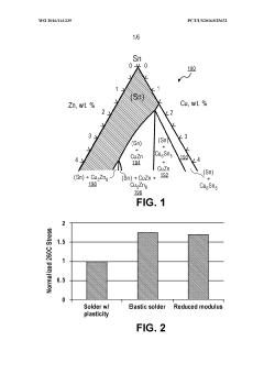
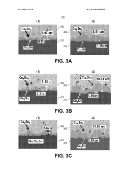
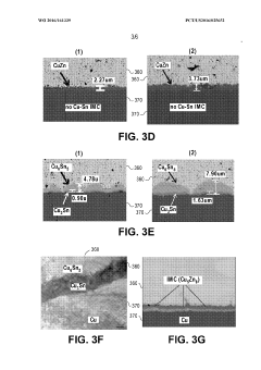
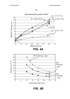
ZN doped solders on CU surface finish for thin FLI application
PatentWO2016161339A1
Innovation
- Incorporating zinc (Zn) into the solder composition to selectively form slower-growing Cu-Zn and Cu6Zn5 IMCs, which act as a barrier layer, reducing the growth of IMCs and minimizing stress on the low-K interlayer dielectric and copper consumption, thereby preventing cracking and allowing for thinner solder joints and increased reflow cycles.
Environmental Impact of Soldering Materials and Processes
The soldering industry faces increasing scrutiny regarding its environmental footprint, particularly concerning the materials and processes involved in creating reliable solder joints. Traditional soldering processes utilize lead-based alloys which pose significant environmental and health hazards. The transition to lead-free alternatives, while addressing toxicity concerns, has introduced new environmental challenges that require comprehensive assessment.
Lead-free solder alloys, predominantly tin-based with additions of silver, copper, and other metals, require higher reflow temperatures, resulting in increased energy consumption during manufacturing. This energy demand translates to higher carbon emissions, particularly in high-volume production environments. Research indicates that optimizing reflow profiles can reduce energy usage by 15-20% while maintaining joint reliability, presenting an opportunity for environmental improvement without compromising product quality.
The formation and control of Intermetallic Compounds (IMCs) during soldering processes also carry environmental implications. Thicker IMCs often result from higher temperature profiles or extended dwell times, both of which increase energy consumption. Additionally, certain IMC formations may affect product longevity, potentially leading to premature electronic waste generation. Studies show that controlling IMC thickness through precise thermal management can extend product lifespan by up to 30%, significantly reducing electronic waste volumes.
Flux residues present another environmental concern in soldering processes. Traditional cleaning methods to remove residual flux often employ volatile organic compounds (VOCs) or water-intensive processes. VOCs contribute to air pollution and potential ozone depletion, while water-based cleaning generates contaminated wastewater requiring treatment. Recent innovations in no-clean flux formulations have reduced cleaning requirements, but these materials may still contain environmentally persistent substances that can leach from disposed electronics.
Life cycle assessments of soldering materials reveal that the environmental impact extends beyond the manufacturing phase. Mining and refining metals for solder alloys, particularly silver and copper, involve significant land disturbance, water usage, and energy consumption. End-of-life considerations are equally important, as improper disposal of electronics can lead to soil and water contamination from leached solder components.
Emerging environmentally conscious approaches include the development of bio-derived flux formulations, energy-efficient reflow technologies, and improved recycling methods for recovering valuable metals from solder joints. These innovations aim to create a more sustainable soldering ecosystem while maintaining the reliability standards necessary for modern electronics.
Reliability Testing Standards and Qualification Methods
Reliability testing standards and qualification methods are essential frameworks for evaluating solder joint performance in electronic assemblies. The industry has established several standardized approaches to ensure consistent assessment of solder joint reliability across different manufacturing environments and applications.
The Joint Electron Device Engineering Council (JEDEC) has developed comprehensive standards such as JESD22-A104 for temperature cycling and JESD22-B110 for mechanical shock testing. These standards define specific test parameters, including temperature ranges, ramp rates, and dwell times that directly correlate with reflow profile optimization research.
IPC standards, particularly IPC-9701 for surface mount solder joint reliability, provide detailed methodologies for testing solder connections under various environmental stresses. These standards incorporate specific guidelines for evaluating the impact of intermetallic compound (IMC) formation on long-term reliability, which is directly relevant to IMC thickness control research.
Thermal cycling tests (TCT) represent a cornerstone of reliability qualification, typically conducted between -40°C and 125°C for consumer electronics, with more stringent ranges for automotive and aerospace applications. The number of cycles to failure provides critical data on how different reflow profiles affect solder joint durability.
Highly accelerated stress testing (HAST) combines elevated temperature and humidity (typically 130°C/85% RH) to evaluate how residual flux compounds might accelerate corrosion mechanisms in solder joints. This test is particularly valuable when investigating the long-term effects of flux residues on electronic assembly reliability.
Drop and vibration testing protocols, standardized under JEDEC JESD22-B111, assess mechanical integrity of solder joints. These tests have revealed significant correlations between IMC thickness and mechanical failure modes, providing valuable insights for IMC control strategies.
Weibull statistical analysis has emerged as the preferred method for interpreting reliability test data, offering characteristic life (η) and shape parameter (β) values that enable quantitative comparison between different solder joint configurations and processing parameters.
Recent developments in reliability testing include the integration of in-situ monitoring techniques, such as electrical resistance measurement during thermal cycling, providing real-time data on crack initiation and propagation in relation to reflow profiles and IMC characteristics.
Unlock deeper insights with Patsnap Eureka Quick Research — get a full tech report to explore trends and direct your research. Try now!
Generate Your Research Report Instantly with AI Agent
Supercharge your innovation with Patsnap Eureka AI Agent Platform!