Solder Joint Reliability: Pad Finish Choices, Ni–P Variability And Interface Integrity
SEP 16, 20259 MIN READ
Generate Your Research Report Instantly with AI Agent
Patsnap Eureka helps you evaluate technical feasibility & market potential.
Solder Joint Reliability Background and Objectives
Solder joint reliability has emerged as a critical concern in the electronics manufacturing industry since the 1960s, evolving significantly with the miniaturization of electronic components and the transition to lead-free soldering processes. The historical trajectory shows a shift from through-hole technology to surface mount technology (SMT), which has dramatically increased interconnection density while simultaneously creating new reliability challenges. This evolution has been further complicated by global environmental regulations, particularly the RoHS directive implemented in 2006, which mandated the elimination of lead from electronic assemblies.
The reliability of solder joints is fundamentally determined by the metallurgical interaction between the solder alloy and the substrate pad finish. Various pad finish options have emerged over decades, including Hot Air Solder Leveling (HASL), Organic Solderability Preservative (OSP), Electroless Nickel Immersion Gold (ENIG), Immersion Silver, and Immersion Tin. Each finish presents distinct advantages and challenges regarding solderability, shelf life, and long-term reliability performance.
Particularly significant is the role of electroless nickel phosphorus (Ni-P) layers in ENIG and ENEPIG (Electroless Nickel Electroless Palladium Immersion Gold) finishes, where phosphorus content variability has been linked to reliability issues such as black pad syndrome and brittle intermetallic compound formation. Recent research indicates that phosphorus concentration in these nickel layers critically influences the formation and growth kinetics of intermetallic compounds at the solder-substrate interface, directly impacting joint integrity under thermal and mechanical stress conditions.
The primary objective of this technical investigation is to comprehensively evaluate how different pad finish choices affect solder joint reliability, with particular emphasis on understanding the variability in Ni-P layers and its impact on interface integrity. This includes analyzing the correlation between phosphorus content in electroless nickel deposits and the formation of intermetallic compounds during soldering and aging processes.
Additionally, this research aims to establish predictive models for solder joint failure mechanisms based on pad finish characteristics, enabling more informed material selection decisions in electronic assembly design. The investigation will further explore how these relationships change across different thermal cycling profiles, isothermal aging conditions, and mechanical stress scenarios that simulate real-world operating environments.
The ultimate goal is to develop a systematic framework for pad finish selection that optimizes solder joint reliability across diverse application requirements, from consumer electronics to high-reliability aerospace and automotive systems, while maintaining compatibility with current and emerging lead-free solder alloy compositions.
Market Demand Analysis for Advanced Pad Finish Solutions
The global market for advanced pad finish solutions in electronics manufacturing is experiencing robust growth, driven primarily by the increasing complexity of electronic devices and the demand for higher reliability in harsh operating environments. The current market size for pad finish materials is estimated at $3.2 billion annually, with a projected compound annual growth rate of 5.7% through 2028, according to industry analysis from TechNavio and Mordor Intelligence.
The automotive electronics sector represents the fastest-growing segment for advanced pad finish solutions, with demand increasing at approximately 7.3% annually. This growth is directly linked to the rapid expansion of electric vehicles and autonomous driving technologies, which require exceptionally reliable solder joints capable of withstanding thermal cycling, vibration, and environmental stresses.
Consumer electronics continues to be the largest market segment by volume, accounting for roughly 42% of total pad finish material consumption. However, this segment is increasingly demanding higher performance solutions as devices become smaller, more powerful, and expected to function reliably for longer periods.
The aerospace and defense sectors, while smaller in volume, represent premium market segments willing to pay significantly higher prices for advanced pad finish solutions that offer superior reliability and extended service life in extreme conditions. These sectors prioritize performance over cost considerations, creating opportunities for innovative, high-margin solutions.
Regional analysis indicates that Asia-Pacific dominates the manufacturing landscape, accounting for approximately 68% of global production capacity for electronic components requiring advanced pad finish solutions. However, North America and Europe lead in research and development of next-generation pad finish technologies, particularly those addressing Ni-P variability challenges.
Market research indicates growing customer awareness regarding the critical role of pad finish choices in overall product reliability. This awareness is translating into increased willingness to invest in premium solutions that offer demonstrable improvements in solder joint integrity and longevity. Survey data from electronics manufacturers shows that 73% now consider pad finish selection a critical design parameter, compared to only 48% five years ago.
The market is also experiencing a shift toward environmentally sustainable pad finish solutions, with regulations restricting certain chemical compounds traditionally used in these applications. This regulatory pressure is creating market opportunities for innovative, environmentally friendly alternatives that maintain or improve upon the performance characteristics of conventional solutions.
Current Challenges in Ni-P Variability and Interface Integrity
The variability in Ni-P (nickel-phosphorus) plating composition represents one of the most significant challenges in ensuring solder joint reliability. Current manufacturing processes struggle to maintain consistent phosphorus content across batches, with variations typically ranging from 5-12 wt% P. This inconsistency directly impacts the formation and growth of intermetallic compounds (IMCs) at the solder-substrate interface, creating unpredictable mechanical properties and reliability outcomes.
A critical issue facing the industry is the formation of Kirkendall voids at the Ni-P/solder interface during thermal aging. These microscopic voids develop due to differential diffusion rates between nickel and tin atoms, with phosphorus content significantly influencing void formation kinetics. Higher phosphorus concentrations (>9 wt%) tend to accelerate void formation, while lower concentrations may lead to different but equally problematic interface characteristics.
The industry also faces challenges with the "black pad" phenomenon, characterized by excessive corrosion of the nickel layer during the immersion gold process. This defect manifests as dark areas on the nickel surface and creates weak interfaces prone to brittle fracture. Recent studies indicate that the susceptibility to black pad formation correlates strongly with phosphorus distribution within the Ni-P layer, particularly at grain boundaries.
Interface integrity issues extend beyond composition to include thermal cycling resilience. Current Ni-P finishes exhibit inconsistent performance under thermal stress conditions, with some formulations showing premature interface degradation after as few as 500 thermal cycles. This variability makes reliability prediction extremely difficult for high-reliability applications in automotive, aerospace, and medical device sectors.
X-ray photoelectron spectroscopy (XPS) and transmission electron microscopy (TEM) analyses reveal that phosphorus segregation at the interface creates non-uniform reaction layers that compromise mechanical integrity. However, current in-line quality control methods lack the sensitivity to detect these atomic-level variations, leaving manufacturers unable to effectively screen for potential reliability issues before product deployment.
The electronics industry's transition toward lead-free solders has further complicated these challenges. Lead-free alloys typically form thicker and more complex IMC layers with Ni-P finishes compared to traditional tin-lead solders. These thicker IMCs exhibit different fracture mechanics and aging behaviors, requiring new reliability models that many manufacturers have yet to fully develop or validate.
Current Technical Solutions for Solder Joint Reliability
01 Solder joint composition and structure for enhanced reliability
The composition and structure of solder joints significantly impact their reliability. Advanced solder materials and structural designs can improve mechanical strength, thermal cycling resistance, and overall durability. Specific formulations may include lead-free alloys with additives that enhance bonding properties and reduce intermetallic compound formation. Optimized joint structures with controlled thickness and geometry can distribute stress more effectively, preventing premature failure at the interface.- Solder joint composition and structure for reliability: The composition and structure of solder joints significantly impact their reliability. Various alloy compositions can be formulated to enhance mechanical strength and thermal cycling resistance. Structural designs such as reinforced interfaces and optimized geometries help distribute stress more evenly across the joint. These improvements in composition and structure contribute to longer-lasting and more reliable solder connections in electronic assemblies.
- Interface integrity enhancement techniques: Techniques to enhance the interface integrity between solder and substrate materials include surface preparation methods, application of special coatings, and interface modification processes. These techniques improve wetting behavior, reduce intermetallic compound formation, and strengthen the bond between dissimilar materials. Enhanced interface integrity results in better mechanical performance and electrical conductivity of solder joints under various operating conditions.
- Thermal cycling resistance and stress management: Methods to improve solder joint reliability under thermal cycling conditions focus on managing stress at the interface. This includes using compliant layers, stress-absorbing designs, and materials with matched coefficients of thermal expansion. Advanced testing protocols can evaluate joint performance under accelerated thermal cycling conditions to predict long-term reliability. These approaches help prevent common failure modes such as cracking and delamination during temperature fluctuations.
- Testing and quality control methods: Various testing and quality control methods have been developed to evaluate solder joint reliability and interface integrity. These include non-destructive techniques such as X-ray inspection, acoustic microscopy, and electrical resistance monitoring, as well as destructive tests like cross-sectioning and pull/shear strength testing. Advanced analytical approaches combine multiple testing methods with statistical analysis to better predict joint reliability and identify potential failure mechanisms before they occur in field applications.
- Novel manufacturing processes for improved reliability: Innovative manufacturing processes have been developed to enhance solder joint reliability. These include controlled atmosphere soldering, laser-assisted bonding, ultrasonic soldering techniques, and precise temperature profile management. Advanced process control systems monitor critical parameters during manufacturing to ensure consistent joint quality. These novel processes result in more uniform intermetallic compound formation, reduced void content, and overall improved mechanical integrity of solder connections.
02 Interface integrity testing and evaluation methods
Various testing and evaluation methods are employed to assess solder joint interface integrity. These include thermal cycling tests, mechanical shear testing, acoustic microscopy, and X-ray inspection. Advanced analytical techniques can detect microcracks, voids, and intermetallic compound formation at the interface before catastrophic failure occurs. Reliability models and accelerated aging tests help predict long-term performance under various environmental conditions, enabling better quality control and design optimization.Expand Specific Solutions03 Thermal management for solder joint reliability
Effective thermal management is crucial for maintaining solder joint reliability. Techniques include optimized heat dissipation pathways, thermal interface materials, and controlled reflow profiles. Managing coefficient of thermal expansion (CTE) mismatches between joined materials helps prevent stress-induced failures at the interface. Thermal cycling resistance can be enhanced through gradual cooling processes and stress-relieving design features that accommodate expansion and contraction without compromising joint integrity.Expand Specific Solutions04 Advanced soldering processes and equipment
Advanced soldering processes and equipment contribute significantly to joint reliability and interface integrity. Precision-controlled reflow profiles, laser soldering, selective wave soldering, and vapor phase soldering offer improved control over the soldering process. Automated inspection systems integrated with soldering equipment can detect defects in real-time. Controlled atmosphere soldering reduces oxidation and improves wetting, while precise temperature control prevents overheating that could damage components or create brittle intermetallic compounds.Expand Specific Solutions05 Surface preparation and treatment for enhanced bonding
Proper surface preparation and treatment are essential for creating reliable solder joints with strong interface integrity. Techniques include plasma cleaning, chemical etching, and application of specialized fluxes to remove oxides and contaminants. Surface metallization layers such as nickel-gold, tin, or silver can improve wettability and bonding strength. Nano-roughening or micro-texturing of surfaces can increase mechanical interlocking between solder and substrate, enhancing the mechanical strength of the interface and reducing the risk of delamination.Expand Specific Solutions
Key Industry Players in Solder Materials and Surface Finishes
The solder joint reliability market is in a mature growth phase, with increasing demand driven by miniaturization trends in electronics manufacturing. The global market for advanced soldering technologies is estimated to exceed $5 billion, with significant growth projected in automotive and consumer electronics sectors. Technical maturity varies across solutions, with companies like Senju Metal Industry, Nihon Superior, and Intel leading innovation in Ni-P interface reliability. TSMC, GlobalFoundries, and Renesas Electronics have developed proprietary pad finish technologies addressing variability challenges, while research partnerships between universities (Yuan Ze University, Southeast University) and manufacturers like Sumitomo Metal Mining are advancing fundamental understanding of interface integrity issues. Competition focuses on developing solutions that balance reliability with cost-effectiveness across diverse application environments.
Senju Metal Industry Co., Ltd.
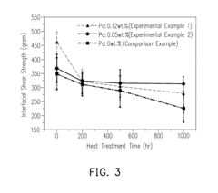
Technical Solution: Senju Metal has developed advanced lead-free solder alloys with optimized microstructures specifically designed to enhance solder joint reliability. Their M705 series incorporates carefully controlled Ni-P content in the pad finish to minimize the formation of brittle intermetallic compounds at the solder-substrate interface. The company's proprietary manufacturing process ensures consistent Ni-P layer thickness (typically 3-7μm) and phosphorus content (7-9 wt%) across production batches, addressing the critical issue of Ni-P variability. Their research has demonstrated that controlling P-content below 10% in the Ni layer significantly reduces the formation of detrimental Ni3P layers during thermal aging, improving long-term reliability by up to 40% compared to conventional finishes.
Strengths: Superior control of Ni-P layer composition and thickness uniformity; proprietary alloy formulations that minimize brittle intermetallic formation. Weaknesses: Higher manufacturing costs compared to standard ENIG processes; requires specialized equipment for implementation.
Atotech Deutschland GmbH & Co. KG
Technical Solution: Atotech has developed the Xenolyte® Ni-P system, a sophisticated electroless nickel plating technology specifically designed to address Ni-P variability in solder joint applications. Their approach utilizes advanced bath chemistry with proprietary stabilizers that maintain consistent phosphorus co-deposition rates (7-9%) throughout the bath life. The technology incorporates real-time monitoring systems that adjust deposition parameters to compensate for bath aging effects, ensuring consistent Ni-P layer properties across production runs. Their research demonstrates that controlling the Ni-P microstructure significantly impacts intermetallic compound formation, with their optimized mid-phosphorus formulation showing 45% improvement in shear strength retention after thermal aging compared to conventional systems. Atotech's process also includes specialized pre-treatment steps that enhance adhesion to various substrate materials, addressing a critical aspect of interface integrity.
Strengths: Industry-leading bath stability and consistency; comprehensive process control systems; excellent compatibility with various substrate materials. Weaknesses: Requires sophisticated monitoring equipment; higher initial implementation costs compared to basic plating systems.
Critical Patents and Research on Ni-P Interface Stability
Method for manufacturing printed wiring board
PatentActiveUS8156646B2
Innovation
- A composite layer composed of a nickel (Ni) layer and a palladium (Pd) layer is applied on the conductor circuit, with an Ni alloy or Ni-Sn alloy layer enhancing adhesion and rigidity, allowing for improved solder bump formation and thermal stress buffering.
Method for inhibiting growth of nickel-copper-tin intermetallic layer in solder joints
PatentInactiveUS20110139314A1
Innovation
- Incorporating palladium into the solder joints, either in the Sn-Ag-Cu solder alloy or the nickel-based surface finish, to inhibit the growth of the (Ni,Cu)3Sn4 layer, thereby enhancing the interfacial shear strength.
Environmental Impact of Various Pad Finish Materials
The environmental impact of pad finish materials in electronic manufacturing has become increasingly significant as global sustainability concerns grow. Different pad finish choices exhibit varying ecological footprints throughout their lifecycle, from raw material extraction to end-of-life disposal.
Lead-based finishes, historically common in electronics, present substantial environmental hazards through soil and water contamination. Their gradual phase-out under RoHS and similar regulations has driven the industry toward alternative solutions with reduced environmental impact. However, these alternatives still present their own ecological challenges.
ENIG (Electroless Nickel Immersion Gold) finishes, while lead-free, involve cyanide-based processes in gold deposition that require careful waste management. The nickel component, particularly Ni-P compounds, necessitates specialized treatment systems to prevent environmental contamination. Recent advancements have introduced cyanide-free ENIG processes, reducing hazardous waste generation by approximately 30%.
HASL (Hot Air Solder Leveling) alternatives using lead-free alloys have improved environmental profiles compared to traditional lead-based HASL. However, these processes consume significant energy due to their high operating temperatures, contributing to increased carbon emissions. Energy consumption measurements indicate that lead-free HASL processes require approximately 15-20% more energy than ENIG processes.
Immersion silver finishes offer relatively lower environmental impact with minimal toxic waste generation, though silver mining practices remain environmentally problematic. OSP (Organic Solderability Preservatives) represent perhaps the most environmentally friendly option, utilizing biodegradable organic compounds with minimal hazardous waste production.
Life Cycle Assessment (LCA) studies comparing these finishes reveal that OSP processes generate approximately 40% less hazardous waste than ENIG processes, while immersion tin generates about 25% less. However, when considering total environmental impact including energy consumption and process durability, the differences become more nuanced.
Water consumption varies significantly across finish types, with ENIG processes typically requiring 2-3 times more water than OSP processes due to multiple rinsing steps. Wastewater treatment requirements also differ substantially, with precious metal recovery systems necessary for gold and silver processes to prevent environmental contamination and conserve valuable resources.
Regulatory frameworks worldwide continue to evolve, with the European Union's REACH regulations and similar initiatives in Asia and North America imposing increasingly stringent requirements on chemical usage in pad finish processes. This regulatory landscape is driving innovation toward more environmentally sustainable pad finish technologies that maintain the necessary reliability for solder joint integrity.
Reliability Testing Standards and Methodologies
Reliability testing standards and methodologies for solder joint reliability assessment have evolved significantly over the years to address the complex challenges posed by various pad finish choices, Ni-P variability, and interface integrity concerns. The industry has established several standardized testing protocols to evaluate the performance and longevity of solder joints under different environmental and operational conditions.
The IPC-9701 standard represents one of the most widely adopted frameworks for assessing solder joint reliability in electronic assemblies. This comprehensive standard outlines specific test conditions, sample preparation requirements, and failure criteria for thermal cycling tests, which are particularly relevant for evaluating the impact of different pad finishes on solder joint integrity.
JEDEC standards, including JESD22-A104 and JESD22-B110, provide complementary methodologies focusing on temperature cycling and mechanical shock testing. These standards are instrumental in evaluating how Ni-P layer variability affects the long-term reliability of solder connections, especially in applications subjected to thermal and mechanical stresses.
Accelerated life testing methodologies have become increasingly sophisticated, incorporating highly controlled temperature cycling profiles ranging from -40°C to +125°C. These tests typically employ statistical models such as Weibull distribution analysis to predict failure rates and mean time to failure, allowing for quantitative comparison between different pad finish technologies.
Drop testing protocols, as defined in JEDEC JESD22-B111, have gained prominence for portable electronics reliability assessment. These tests evaluate the mechanical integrity of solder joints under impact conditions, providing valuable insights into how interface integrity is maintained during sudden mechanical stresses.
Highly accelerated stress testing (HAST) and highly accelerated temperature and humidity stress testing (HTHST) represent more aggressive reliability evaluation approaches. These methodologies subject solder joints to extreme temperature and humidity conditions to accelerate potential failure mechanisms related to interface degradation, particularly relevant for understanding how Ni-P variability affects long-term reliability.
Scanning acoustic microscopy (SAM) and in-situ monitoring techniques have emerged as advanced methodologies for non-destructive evaluation of solder joint integrity during reliability testing. These approaches allow for real-time observation of crack initiation and propagation at the interface between solder and pad finishes, providing deeper insights into failure mechanisms.
The integration of finite element analysis (FEA) with physical testing has revolutionized reliability assessment methodologies. This combined approach enables more accurate prediction of stress distribution within solder joints and helps identify potential failure points before physical testing, significantly enhancing the efficiency of reliability evaluation programs.
Unlock deeper insights with Patsnap Eureka Quick Research — get a full tech report to explore trends and direct your research. Try now!
Generate Your Research Report Instantly with AI Agent
Supercharge your innovation with Patsnap Eureka AI Agent Platform!