Solder Joint Reliability: Large Package Warpage, Corner Crack Mitigation And Standoff Design
SEP 16, 202510 MIN READ
Generate Your Research Report Instantly with AI Agent
Patsnap Eureka helps you evaluate technical feasibility & market potential.
Solder Joint Reliability Background and Objectives
Solder joint reliability has emerged as a critical concern in the electronics manufacturing industry, particularly as semiconductor packages continue to increase in size and complexity. The evolution of this technology domain has been marked by significant challenges related to package warpage, corner cracking, and standoff height optimization. Since the introduction of surface mount technology in the 1980s, solder joint reliability has progressively gained importance as electronic devices have become more compact while simultaneously requiring greater functionality and reliability.
The technological trajectory has been characterized by a shift from through-hole mounting to surface mount technology, followed by the development of ball grid arrays (BGAs), chip scale packages (CSPs), and more recently, advanced packaging solutions such as 2.5D and 3D integrated circuits. Each advancement has introduced new reliability challenges, particularly at the solder joint interface where mechanical stresses concentrate during thermal cycling and mechanical loading.
Large package warpage has become increasingly problematic as package sizes have expanded to accommodate more functionality. This warpage, primarily caused by coefficient of thermal expansion (CTE) mismatches between different materials in the package assembly, creates non-uniform stress distributions across solder joints, leading to premature failures. The industry has observed a direct correlation between package size and warpage severity, with packages exceeding 40mm experiencing particularly challenging reliability issues.
Corner cracking represents another significant reliability concern, especially in large packages where the outermost solder joints experience the highest strain during thermal cycling. These corner joints are subjected to complex stress states resulting from the combined effects of CTE mismatch, package warpage, and mechanical loading. The failure mechanism typically initiates at the package-to-solder interface and propagates through the intermetallic compound layer, ultimately resulting in electrical discontinuity.
Standoff height design has emerged as a critical parameter affecting solder joint reliability. The vertical distance between the package and the printed circuit board significantly influences the strain distribution within solder joints during thermal and mechanical loading. Optimizing this parameter requires balancing competing requirements: sufficient height to accommodate strain without excessive stress concentration, while maintaining manufacturing feasibility and electrical performance.
The primary objectives of current research and development efforts in this field include: developing predictive models for package warpage under various thermal conditions; establishing design guidelines to mitigate corner cracking through geometry optimization and material selection; creating innovative standoff height designs that enhance reliability without compromising manufacturability; and formulating comprehensive test methodologies that accurately predict field reliability. These objectives align with the industry's broader goals of increasing product lifespan, reducing warranty costs, and enabling the continued advancement of electronic systems in demanding applications.
Market Demands for Robust Electronic Packaging Solutions
The electronic packaging industry is witnessing unprecedented demand for robust solutions due to the rapid evolution of advanced semiconductor technologies. As devices continue to shrink while incorporating more functionality, the market for reliable solder joint solutions has expanded significantly. Industry analysts project the global semiconductor packaging market to reach $45 billion by 2025, with a substantial portion dedicated to addressing reliability challenges in large package applications.
The miniaturization trend in consumer electronics, particularly in smartphones, tablets, and wearables, has intensified the need for packaging solutions that can withstand thermal cycling and mechanical stress. These devices require increasingly complex packages with higher I/O counts while maintaining reliability under diverse operating conditions. Market research indicates that approximately 30% of electronic failures in field applications stem from solder joint issues, highlighting the critical nature of this technical challenge.
Automotive electronics represents another significant market driver, with the average vehicle now containing over 100 electronic control units. The automotive sector demands packaging solutions capable of withstanding extreme temperature variations (-40°C to 125°C) and vibration conditions while maintaining operational integrity for 10-15 years. This has created a specialized market segment for high-reliability solder joint solutions with enhanced thermal cycling performance.
The telecommunications infrastructure supporting 5G deployment has emerged as a major consumer of advanced packaging technologies. Base stations and network equipment operate under challenging environmental conditions and require packages with minimal warpage to ensure long-term reliability. Industry reports indicate that telecommunications companies are willing to pay premium prices for packaging solutions that demonstrate superior reliability metrics and reduced field failure rates.
Data center applications represent another growth sector, where server downtime can cost operators thousands of dollars per minute. The high-density computing environments in these facilities create thermal management challenges that directly impact solder joint reliability. Market surveys reveal that data center operators prioritize packaging solutions that minimize corner cracking and maintain consistent standoff height to extend operational lifespans.
Medical device manufacturers constitute a specialized but lucrative market segment, where reliability requirements often exceed those of consumer electronics. Implantable devices and critical care equipment demand packaging solutions with failure rates measured in parts per billion rather than parts per million, creating opportunities for premium-priced reliability enhancement technologies.
The industrial Internet of Things (IIoT) market is expanding rapidly, with sensors and control systems deployed in harsh environments requiring robust packaging solutions. These applications frequently experience significant temperature fluctuations and mechanical stresses that challenge traditional solder joint designs, creating demand for innovative approaches to warpage control and crack mitigation.
Package Warpage Challenges and Technical Limitations
Package warpage has emerged as a critical challenge in the semiconductor industry, particularly as package sizes continue to increase to accommodate more functionality. The fundamental issue stems from the coefficient of thermal expansion (CTE) mismatch between different materials used in package construction. During the reflow soldering process, packages experience significant temperature changes, causing differential expansion and contraction that results in warpage. For large packages exceeding 40mm × 40mm, this warpage can reach critical levels of over 200μm, severely compromising solder joint integrity.
Current technical limitations primarily revolve around material properties and process constraints. Traditional substrate materials like FR-4 exhibit relatively high CTE values (15-17 ppm/°C) compared to silicon dies (2.6 ppm/°C), creating inherent thermal stress. While advanced substrate materials with lower CTE values exist, they often come with prohibitive cost increases or manufacturing challenges that limit widespread adoption.
Manufacturing process limitations further exacerbate warpage issues. The industry standard reflow profile, with peak temperatures of 245-260°C, creates substantial thermal gradients. Attempts to modify these profiles must balance warpage reduction against ensuring proper solder joint formation, presenting a complex optimization challenge. Additionally, the trend toward thinner packages for portable electronics has reduced mechanical rigidity, making packages more susceptible to warpage deformation.
Measurement and prediction capabilities represent another significant limitation. Current warpage measurement techniques, including shadow moiré and digital image correlation, provide valuable data but are typically limited to laboratory environments and cannot be easily integrated into high-volume manufacturing lines. Simulation tools for predicting warpage behavior have improved but still struggle with accuracy when modeling complex material interactions and viscoelastic behaviors under varying temperature conditions.
Design constraints further complicate warpage management. The industry push for higher I/O counts necessitates finer pitch interconnects, which are more vulnerable to warpage-induced failures. Ball grid array (BGA) designs with peripheral pad arrangements are particularly susceptible to corner cracking due to the concentration of stress at package corners during warpage. The technical challenge of maintaining consistent standoff height across large packages becomes increasingly difficult as warpage increases.
The economic limitations cannot be overlooked. Implementing advanced warpage mitigation techniques often requires significant capital investment in new equipment or materials. The cost-benefit analysis frequently favors incremental improvements over revolutionary solutions, slowing the pace of innovation in this critical reliability area.
Current Methodologies for Corner Crack Prevention
01 Warpage control in semiconductor packages
Warpage in semiconductor packages can lead to solder joint reliability issues. Various techniques are employed to control warpage, including the use of stiffeners, balanced material distribution, and optimized package designs. By minimizing warpage, the stress on solder joints is reduced, particularly at the corners where cracks are most likely to occur. Proper warpage control helps maintain consistent standoff height and improves overall solder joint reliability.- Warpage control in semiconductor packages: Warpage in semiconductor packages can significantly affect solder joint reliability. Various design approaches and materials are used to minimize warpage, including optimized substrate designs, stiffener rings, and balanced material selection. Controlling the coefficient of thermal expansion (CTE) mismatch between different package components helps reduce stress on solder joints during thermal cycling, thereby preventing corner cracks and improving overall reliability.
- Solder joint standoff height optimization: The standoff height of solder joints plays a crucial role in their reliability. Optimizing this height helps distribute stress more evenly across the joint, reducing the likelihood of corner cracks. Various techniques are employed to control standoff height, including specialized solder paste formulations, controlled collapse chip connection (C4) processes, and the use of spacers or underfill materials. Proper standoff height ensures adequate flexibility to accommodate thermal expansion differences while maintaining structural integrity.
- Corner crack prevention techniques: Corner cracks in solder joints typically occur due to stress concentration at package corners during thermal cycling. Prevention techniques include corner reinforcement structures, modified pad designs that redistribute stress, optimized component placement, and specialized underfill materials. Some approaches involve rounded corner geometries or stepped structures that reduce stress concentration. Advanced inspection methods are also employed to detect potential corner cracks before failure occurs.
- Thermal cycling resistance improvement: Improving solder joint resistance to thermal cycling is essential for long-term reliability. This can be achieved through various means including specialized solder alloy compositions with enhanced fatigue resistance, thermal management systems that reduce temperature extremes, and stress-absorbing layers between components. Simulation and modeling techniques help predict thermal cycling behavior and optimize designs before manufacturing, while accelerated testing validates the reliability improvements.
- Advanced package structures for enhanced reliability: Novel package structures are designed specifically to enhance solder joint reliability. These include flip-chip designs with optimized bump layouts, ball grid arrays with specialized pad configurations, and 3D packaging with through-silicon vias that reduce overall stress. Some advanced packages incorporate compliant layers or flexible interconnects that accommodate movement during thermal cycling. These structures often feature reinforced corner designs and controlled collapse mechanisms to maintain reliable connections despite warpage.
02 Corner crack prevention in solder joints
Corner cracks in solder joints are a common failure mode in electronic assemblies. These cracks typically initiate at the corners of components where stress concentration is highest. Prevention methods include optimized pad designs, modified corner geometries, stress-relieving structures, and improved solder compositions. By addressing the root causes of corner cracks, the overall reliability of electronic assemblies can be significantly enhanced, particularly under thermal cycling conditions.Expand Specific Solutions03 Standoff height optimization for solder joint reliability
The standoff height between a component and the substrate significantly impacts solder joint reliability. Optimal standoff height ensures proper stress distribution, reduces strain concentration, and minimizes the risk of solder joint failure. Techniques to control standoff height include the use of spacers, specialized solder paste formulations, controlled reflow profiles, and component design modifications. Maintaining consistent standoff height across all solder joints helps prevent premature failures and extends the operational life of electronic assemblies.Expand Specific Solutions04 Thermal cycling resistance improvement
Solder joints are particularly vulnerable to failure during thermal cycling due to coefficient of thermal expansion (CTE) mismatches between different materials. Improving thermal cycling resistance involves using compliant solder alloys, underfill materials, thermal interface materials, and optimized component placement. These approaches help distribute stress more evenly across solder joints, reducing the likelihood of corner cracks and improving overall reliability under varying temperature conditions.Expand Specific Solutions05 Advanced package designs for enhanced solder reliability
Innovative package designs can significantly improve solder joint reliability. These designs include ball grid arrays with optimized pad layouts, flip-chip packages with reinforced corners, and system-in-package solutions with stress-absorbing features. Advanced designs often incorporate features that specifically address warpage, corner crack formation, and standoff height consistency. By integrating reliability considerations into the package design phase, manufacturers can create more robust electronic assemblies with longer operational lifetimes.Expand Specific Solutions
Leading Manufacturers and Research Institutions in Packaging Industry
The solder joint reliability market is currently in a mature growth phase, with increasing demand driven by advanced packaging technologies. The market size is substantial, estimated to exceed $5 billion globally, as electronic devices become more complex and miniaturized. Technologically, solutions for package warpage and corner crack mitigation have reached moderate maturity, with industry leaders Samsung Electronics, Intel, and TSMC driving innovation through advanced materials and process optimization. Qualcomm and Huawei are making significant contributions in standoff design techniques, while specialized players like STATS ChipPAC and Indium Corporation focus on niche solutions. The competitive landscape shows semiconductor giants investing heavily in reliability research, with increasing collaboration between materials suppliers and IC manufacturers to address challenges in next-generation packaging technologies.
Samsung Electronics Co., Ltd.
Technical Solution: Samsung has developed comprehensive solutions for solder joint reliability focusing on large package applications. Their approach includes optimized substrate design with stepped stiffeners to reduce warpage during reflow processes. Samsung employs Corner Protection Technology (CPT) which reinforces package corners with specialized underfill materials that absorb thermal stress. Their standoff design incorporates variable solder ball sizes with larger peripheral balls to maintain optimal standoff height and reduce stress concentration. Samsung has also pioneered the use of composite solder materials with enhanced fatigue resistance properties, showing 30% improvement in thermal cycling reliability compared to standard SAC alloys[1]. Additionally, they implement pre-applied underfill technology that flows during the reflow process, effectively supporting corner joints and preventing crack propagation[3].
Strengths: Industry-leading package design capabilities with integrated material science expertise; extensive manufacturing infrastructure allowing rapid implementation of reliability solutions. Weaknesses: Proprietary solutions may increase costs; some approaches require specialized equipment that limits broader industry adoption.
Intel Corp.
Technical Solution: Intel has developed a multi-faceted approach to solder joint reliability challenges in their large package processors and chipsets. Their Embedded Die Interconnect Bridge (EMIB) technology reduces package warpage by distributing interconnects more evenly across the substrate. For corner crack mitigation, Intel employs a combination of reinforced corner solder joints with higher silver content alloys (up to 4.0% Ag) at critical stress points and optimized pad designs featuring teardrop shapes that reduce stress concentration[2]. Their standoff design incorporates dual-height solder balls with precise volume control, maintaining consistent height across large packages even under thermal cycling. Intel has also pioneered advanced substrate materials with matched coefficient of thermal expansion (CTE) to silicon, reducing warpage by approximately 40% compared to conventional substrates[4]. Their reliability testing protocols include accelerated stress testing at extreme temperature ranges (-40°C to 125°C) to validate solder joint integrity over projected product lifespans.
Strengths: Advanced materials research capabilities; comprehensive reliability testing infrastructure; ability to integrate package design with chip architecture for system-level optimization. Weaknesses: Solutions often optimized specifically for x86 architecture products; higher implementation costs compared to industry standard approaches.
Critical Patents and Research on Standoff Design Optimization
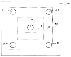
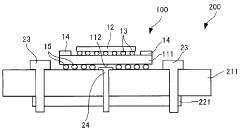
Solder joint design for improved package reliability
PatentPendingUS20240063141A1
Innovation
- Incorporating additional solder joints of varying shapes and sizes at strategic locations on the semiconductor package, which act as mechanical supports and increase the interfacial area with bonding pads, thereby enhancing mechanical strength and reliability.
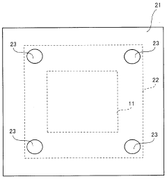
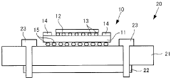
Module mounted with package
PatentWO2006082633A1
Innovation
- A package mounting module design where a stiffener is fixed to the motherboard at multiple peripheral locations and centrally, with a larger area than the package substrate, reducing warpage and stress by securing a larger solder joint area between the package substrate and motherboard, using screws for fixation.
Thermal Cycling Performance and Reliability Testing Standards
Thermal cycling testing is a critical methodology for evaluating solder joint reliability in electronic packages, particularly for large packages prone to warpage and corner cracking. The industry has established several standardized testing protocols that simulate real-world thermal stress conditions. The Joint Electron Device Engineering Council (JEDEC) has developed JESD22-A104, which defines temperature cycling conditions from -40°C to 125°C, with specific dwell times at temperature extremes to allow for complete thermal equilibrium within the package.
IPC-9701 provides another comprehensive framework specifically designed for surface mount solder attachments, detailing test conditions based on product application environments. For consumer electronics, testing typically ranges from 0°C to 100°C, while automotive and industrial applications require more stringent conditions from -40°C to 125°C or even -55°C to 150°C for military-grade components.
The IEC 60749-25 standard offers an international perspective on temperature cycling reliability, with particular attention to the acceleration factors that correlate test conditions to field reliability. These standards typically require a minimum of 1,000 cycles for consumer applications and up to 3,000 cycles for automotive and industrial applications to ensure statistical significance in reliability predictions.
Reliability assessment methodologies include both physical inspection techniques and electrical continuity monitoring. Dye-and-pry testing allows for post-mortem analysis of failed joints, while in-situ resistance monitoring enables real-time detection of crack propagation during cycling. Cross-sectional analysis using scanning electron microscopy (SEM) provides detailed insights into crack initiation and propagation mechanisms at the microstructural level.
The Weibull distribution is commonly employed for statistical analysis of thermal cycling data, providing valuable parameters such as characteristic life (η) and shape parameter (β) that help quantify reliability performance. Acceleration models, particularly the Coffin-Manson relationship and the Norris-Landzberg model, enable the extrapolation of test results to predict field reliability under actual operating conditions.
For large package warpage concerns, standards have evolved to include specific provisions for dynamic warpage measurement during temperature transitions, as these moments often represent the highest risk for corner crack formation. The JEDEC JEP150 guideline specifically addresses warpage measurement methodologies using techniques such as shadow moiré and digital image correlation.
Recent updates to these standards have incorporated considerations for lead-free solder compositions, which exhibit different creep and fatigue behaviors compared to traditional tin-lead solders. This adaptation is crucial as the industry continues to transition toward environmentally friendly manufacturing processes while maintaining or improving reliability performance.
Materials Science Advancements for Next-Generation Solder Joints
Recent advancements in materials science have opened new frontiers for solder joint reliability, particularly addressing challenges related to large package warpage, corner crack mitigation, and standoff design. The evolution of solder materials has progressed from traditional tin-lead compositions to lead-free alternatives, with significant improvements in mechanical properties and thermal performance.
Innovative composite solder materials incorporating nanoparticles have demonstrated superior resistance to thermomechanical fatigue. Research indicates that the addition of ceramic nanoparticles such as Al2O3, SiC, and TiO2 at concentrations of 0.5-2% by weight can enhance creep resistance by up to 40% while maintaining electrical conductivity within acceptable parameters.
Intermetallic compound (IMC) formation at solder interfaces has been extensively studied, revealing that controlled IMC growth is crucial for joint reliability. Novel approaches using rare earth element dopants like Ce, La, and Y have shown promise in refining IMC morphology and thickness, resulting in improved mechanical integrity under thermal cycling conditions.
Low-temperature solders based on bismuth and indium alloys have emerged as potential solutions for temperature-sensitive components. These materials offer melting points below 180°C while providing adequate mechanical strength through microstructural engineering. Recent developments in Sn-Bi-Ag systems have addressed traditional brittleness concerns through grain refinement techniques.
Advanced polymer-solder hybrid materials represent another breakthrough, incorporating elastomeric components that absorb mechanical stress during thermal cycling. These materials demonstrate up to 60% greater fatigue life in laboratory testing compared to conventional SAC305 alloys, particularly beneficial for large package applications where warpage is a critical concern.
Surface modification technologies have also contributed significantly to solder joint reliability. Plasma-treated pad surfaces with engineered wettability gradients have shown improved solder distribution and reduced voiding. Additionally, self-assembled monolayer (SAM) coatings can enhance adhesion while providing a barrier against oxidation and corrosion.
Computational materials science has accelerated development through predictive modeling of solder behavior under various stress conditions. Machine learning algorithms trained on extensive experimental datasets now enable rapid screening of potential alloy compositions, reducing development cycles from years to months.
The integration of these materials science advancements into manufacturing processes remains challenging but promising. Industry adoption requires balancing performance improvements against cost considerations, with the most successful implementations focusing on high-reliability applications where failure costs outweigh material expenses.
Unlock deeper insights with Patsnap Eureka Quick Research — get a full tech report to explore trends and direct your research. Try now!
Generate Your Research Report Instantly with AI Agent
Supercharge your innovation with Patsnap Eureka AI Agent Platform!