How To Tackle Artifacts In Atomic Force Microscopy Imaging — Solutions
SEP 19, 20259 MIN READ
Generate Your Research Report Instantly with AI Agent
PatSnap Eureka helps you evaluate technical feasibility & market potential.
AFM Imaging Artifacts Background and Objectives
Atomic Force Microscopy (AFM) has revolutionized surface characterization since its invention in 1986 by Binnig, Quate, and Gerber. This powerful technique enables three-dimensional imaging of surfaces with nanometer-scale resolution under various environmental conditions, making it invaluable across scientific disciplines from materials science to biological research. Despite its capabilities, AFM imaging frequently suffers from artifacts that can significantly compromise data quality and interpretation.
Artifacts in AFM imaging arise from multiple sources including tip-sample interactions, environmental factors, instrumental limitations, and operational parameters. These distortions represent a persistent challenge that has evolved alongside the technology itself. Early AFM systems struggled with basic feedback loop stability and probe quality issues, while modern systems face more subtle artifacts related to high-speed scanning, complex sample environments, and advanced measurement modes.
The technological evolution of AFM has been marked by continuous improvements in probe manufacturing, detection systems, and control algorithms. From the initial contact mode operations to the development of dynamic modes like tapping and non-contact AFM, each advancement has addressed certain artifacts while sometimes introducing new challenges. Recent developments in high-speed AFM and multifrequency techniques have further expanded capabilities while requiring more sophisticated artifact management strategies.
Current research indicates that approximately 60-70% of published AFM images contain some form of artifact, with tip-induced distortions being the most prevalent. These artifacts not only affect dimensional measurements but can also lead to misinterpretation of surface properties and false identification of structural features. The economic impact is substantial, with research institutions and industries investing significant resources in artifact correction and repeated measurements.
The primary objective of this technical investigation is to comprehensively catalog and analyze the various artifacts encountered in AFM imaging across different operational modes and sample types. We aim to develop a systematic framework for artifact identification, prevention, and correction that can be implemented across research and industrial applications. Additionally, we seek to evaluate emerging computational and instrumental approaches that show promise in minimizing artifacts during data acquisition or through post-processing.
This report will establish a foundation for understanding the fundamental mechanisms behind AFM artifacts, providing both theoretical insights and practical solutions. By addressing these challenges, we anticipate enabling more reliable nanoscale measurements that will advance numerous fields dependent on accurate surface characterization, from semiconductor manufacturing to pharmaceutical development and fundamental materials research.
Market Analysis for High-Precision AFM Solutions
The global market for high-precision Atomic Force Microscopy (AFM) solutions has experienced significant growth in recent years, driven by increasing demand for nanoscale imaging and measurement capabilities across various industries. The market size for AFM equipment was valued at approximately $570 million in 2022 and is projected to reach $850 million by 2028, representing a compound annual growth rate of 6.8%.
The semiconductor industry remains the largest consumer of high-precision AFM solutions, accounting for nearly 35% of the total market share. This dominance is attributed to the continuous miniaturization of semiconductor devices and the increasing complexity of integrated circuits, which require advanced imaging techniques for quality control and failure analysis.
Materials science research represents the second-largest market segment, constituting about 25% of the total market. The growing interest in nanomaterials, thin films, and surface modifications has significantly boosted the demand for artifact-free AFM imaging in this sector.
Life sciences and pharmaceutical industries have emerged as rapidly growing segments, currently representing approximately 20% of the market. The ability to image biological samples at the nanoscale without artifacts has become crucial for drug development, cellular research, and biomaterial characterization.
Regional analysis indicates that North America leads the market with a 38% share, followed by Asia-Pacific (32%) and Europe (25%). The Asia-Pacific region, particularly China, Japan, and South Korea, is expected to witness the highest growth rate due to increasing investments in semiconductor manufacturing and nanotechnology research.
Customer segmentation reveals that academic and research institutions account for 40% of end-users, while industrial applications constitute 60%. Within industrial applications, quality control and R&D departments are the primary users of high-precision AFM solutions.
Price sensitivity varies significantly across different market segments. While academic institutions are more price-sensitive and often opt for more affordable solutions with essential features, industrial customers prioritize precision, reliability, and after-sales support, showing willingness to invest in premium solutions that minimize imaging artifacts.
The market for AFM accessories and software specifically designed to address imaging artifacts has grown at an even faster rate of 8.5% annually, indicating increasing awareness about artifact-related challenges and a growing demand for comprehensive solutions rather than just hardware.
Customer surveys indicate that artifact reduction capabilities now rank among the top three purchasing criteria for new AFM systems, alongside resolution and ease of use, highlighting the critical importance of addressing this technical challenge for market success.
Current Challenges in AFM Imaging Technology
Atomic Force Microscopy (AFM) has revolutionized nanoscale imaging since its invention in 1986, yet despite technological advancements, researchers continue to face significant challenges that limit imaging quality and data reliability. The primary challenge remains artifact identification and mitigation, which requires sophisticated understanding of both instrument mechanics and sample properties.
Tip-sample interaction artifacts represent one of the most persistent issues in AFM imaging. When the probe tip interacts with the sample surface, various forces including van der Waals, electrostatic, and capillary forces can distort measurements. These interactions often produce false topographical features that do not represent the actual sample structure, particularly problematic when imaging soft biological samples or materials with significant surface charge.
Thermal drift poses another substantial challenge, causing gradual displacement between the tip and sample during measurement. This drift introduces systematic errors in image acquisition, especially during high-resolution or time-series imaging where even nanometer-scale movements can significantly compromise data quality. Current thermal compensation algorithms provide only partial solutions to this fundamental physical limitation.
Scanner nonlinearities and hysteresis effects continue to plague AFM systems despite advances in piezoelectric technology. These inherent properties of piezoelectric scanners result in positional inaccuracies that distort image geometry, particularly at the edges of scan ranges or during large-area imaging. While calibration procedures exist, they require frequent repetition and cannot completely eliminate these artifacts.
Feedback loop optimization remains challenging, especially when imaging samples with significant height variations or complex topographies. Improper feedback settings lead to common artifacts such as overshooting, ringing, and parachuting effects that mask true surface features. The optimal parameters vary significantly between different sample types, requiring constant adjustment and expertise.
Environmental factors including vibration, acoustic noise, and electromagnetic interference continue to affect AFM performance despite isolation systems. These external disturbances introduce random noise patterns that reduce image resolution and reliability, particularly problematic for sub-nanometer measurements where signal-to-noise ratio becomes critical.
Tip degradation during scanning represents another significant challenge, as tip geometry directly influences image resolution and artifact formation. Tips can become contaminated, damaged, or blunted during measurement, causing gradual or sudden changes in imaging quality that may not be immediately apparent to operators, leading to misinterpretation of results.
Cross-talk between measurement channels in multimodal AFM techniques adds another layer of complexity, where signals from different measurement modes can interfere with each other, creating artifacts that are particularly difficult to identify and correct without advanced signal processing techniques.
Leading Manufacturers and Research Groups in AFM Technology
Atomic Force Microscopy (AFM) imaging artifacts represent a significant technical challenge in the rapidly evolving nanoscale imaging market. The industry is currently in a growth phase, with the global AFM market expected to reach $1 billion by 2025. Leading players like Bruker Nano, Inc. and Keysight Technologies have developed advanced solutions to address common artifacts through hardware innovations and software algorithms. Research institutions including Brookhaven Science Associates and University of Oregon are contributing fundamental research, while companies such as Applied Materials and GLOBALFOUNDRIES are integrating AFM quality control into semiconductor manufacturing. The technology is approaching maturity in research applications but remains in development for industrial implementation, with emerging players like Artidis AG exploring novel biomedical applications.
Bruker Nano, Inc.
Technical Solution: Bruker Nano has developed comprehensive solutions for addressing artifacts in atomic force microscopy (AFM) imaging through their PeakForce Tapping technology. This proprietary approach controls the maximum force applied to the sample during imaging, significantly reducing lateral forces that cause sample damage and image artifacts. Their system incorporates real-time force curve analysis at each pixel, allowing for automatic parameter optimization that minimizes common artifacts such as tip-sample adhesion effects and feedback errors. Bruker's ScanAsyst technology further enhances this capability by continuously monitoring image quality and automatically adjusting scanning parameters to maintain optimal imaging conditions. For addressing thermal drift artifacts, Bruker implements closed-loop scanners with position sensors that provide real-time correction of piezo nonlinearities and hysteresis. Their latest AFM systems also feature advanced noise isolation systems that effectively reduce vibrational artifacts, particularly important for high-resolution imaging applications.
Strengths: Industry-leading force control technology that significantly reduces common AFM artifacts; automated parameter optimization reduces user dependency; integrated hardware and software solutions address multiple artifact sources simultaneously. Weaknesses: Premium pricing may limit accessibility for some research groups; proprietary technologies create potential vendor lock-in; some automated correction systems may occasionally over-process data.
Keysight Technologies, Inc.
Technical Solution: Keysight Technologies has developed the Scanning Microwave Microscopy (SMM) technology that addresses several common artifacts in atomic force microscopy imaging. Their approach integrates vector network analyzer capabilities with AFM technology, allowing simultaneous acquisition of topographical and electrical property data while minimizing cross-talk artifacts between these measurement channels. Keysight's systems feature advanced digital PID controllers that significantly reduce feedback-related artifacts by optimizing the response time to topographical changes. For addressing tip-sample interaction artifacts, their Quick Sense technology enables rapid force curve measurements at each pixel, allowing real-time adjustment of contact parameters to maintain consistent imaging conditions. Keysight has also implemented sophisticated drift correction algorithms in their NanoNavigator software that can compensate for both thermal and mechanical drift during long imaging sessions. Their systems incorporate active vibration isolation platforms that effectively minimize environmental vibration artifacts, particularly important for high-resolution imaging in challenging environments.
Strengths: Unique integration of microwave and AFM technologies provides artifact-reduced multimodal imaging; sophisticated digital control systems minimize feedback artifacts; comprehensive software suite for artifact identification and correction. Weaknesses: Complex technology requires significant expertise to optimize; higher initial investment compared to standard AFM systems; specialized probes needed for optimal performance increase operational costs.
Critical Patents and Research on AFM Imaging Enhancement
Atomic force microscopy true shape measurement method
PatentInactiveUS8296860B2
Innovation
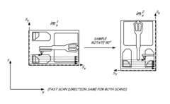
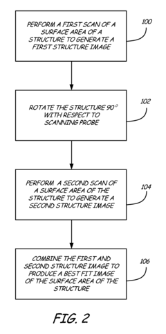
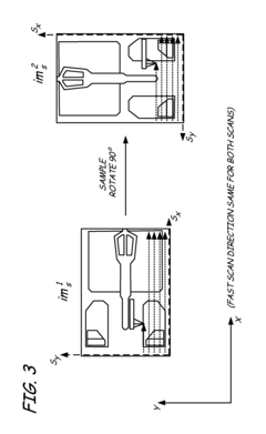
- The method involves scanning a structure and a flat standard surface twice, each time rotated 90°, and combining the images to produce best fit images. These best fit images are then subtracted to eliminate thermal drift and Zrr errors, allowing for the generation of a true topographical image.
Method and apparatus for performing atomic force microscopy measurements
PatentInactiveUS6823723B2
Innovation
- A method and apparatus that modulate the force profile during scanning, allowing the probe tip to maintain contact with varying forces, enabling simultaneous electrical and topographical data collection by defining a force profile with periodic high and low force levels, and optionally a speed profile, to minimize tip damage and optimize data acquisition.


Calibration Standards and Quality Control in AFM Imaging
Calibration standards and quality control mechanisms are essential components in ensuring reliable and artifact-free Atomic Force Microscopy (AFM) imaging. The implementation of standardized calibration protocols significantly reduces measurement uncertainties and enhances the reproducibility of AFM data across different instruments and laboratories.
Primary calibration standards for AFM include silicon gratings with precisely defined step heights, pitch distances, and geometric patterns. These standards enable accurate calibration of the x, y, and z axes, ensuring dimensional measurements remain consistent and traceable to international standards. Commercially available calibration grids, such as those manufactured by Bruker, NT-MDT, and MikroMasch, provide reference structures with certified dimensions that allow operators to verify scanner performance and correct for nonlinearities.
Regular calibration procedures should address three critical aspects of AFM operation: piezoelectric scanner calibration, cantilever spring constant determination, and tip characterization. Scanner calibration corrects for hysteresis, creep, and cross-coupling effects that can introduce significant artifacts in imaging. Modern AFM systems incorporate closed-loop feedback mechanisms that continuously monitor scanner position using capacitive or optical sensors, substantially reducing positional errors.
Quality control in AFM imaging extends beyond initial calibration to include ongoing performance verification. Establishing standard operating procedures (SOPs) for routine instrument checks helps maintain imaging quality over time. These procedures typically include periodic measurements of reference samples to track instrument drift, sensitivity changes, and tip wear. Statistical process control methods can be applied to monitor key performance metrics and detect deviations before they impact research outcomes.
Tip qualification represents another crucial aspect of AFM quality control. Blind tip reconstruction algorithms enable the characterization of tip geometry from images of sharp features, allowing operators to assess tip condition without direct visualization. Implementing tip qualification protocols before critical measurements ensures that artifacts arising from tip asymmetry or contamination are identified and addressed promptly.
Documentation of calibration history and quality control metrics provides valuable data for troubleshooting and validates the reliability of research findings. Modern AFM systems increasingly incorporate automated calibration routines and quality assurance software that streamline these processes and maintain comprehensive records of instrument performance. These tools enable researchers to establish confidence intervals for their measurements and quantitatively assess data quality.
Environmental Factors Affecting AFM Measurement Accuracy
Atomic Force Microscopy (AFM) measurements are highly sensitive to environmental conditions, which can significantly impact the accuracy and reliability of imaging results. Temperature fluctuations represent one of the most critical environmental factors affecting AFM performance. Even minor temperature variations can cause thermal drift in the scanning system, resulting in image distortion and measurement inaccuracies. This thermal instability affects both the sample and the instrument components, leading to dimensional changes that compromise precision.
Humidity levels similarly play a crucial role in AFM measurement accuracy. Excessive humidity can create water films on sample surfaces, particularly affecting hydrophilic materials, which interferes with tip-sample interactions and distorts topographical data. Conversely, extremely low humidity environments may generate problematic static charges that influence the cantilever behavior and introduce artifacts in the resulting images.
Acoustic vibrations from the surrounding environment constitute another significant challenge for AFM systems. External noise sources such as laboratory equipment, HVAC systems, and even human conversation can transmit mechanical vibrations through air or structural pathways to the AFM apparatus. These vibrations manifest as periodic noise patterns in images, obscuring true surface features and limiting resolution capabilities.
Electromagnetic interference (EMI) from nearby electronic devices, power lines, or laboratory equipment can severely compromise AFM measurements. The sensitive electronic components in AFM systems can detect and amplify these electromagnetic disturbances, introducing noise patterns that degrade image quality and measurement precision. Particularly problematic are high-frequency EMI sources that can directly interfere with the AFM's detection systems.
Air quality and particulate contamination represent additional environmental concerns. Airborne particles can settle on samples or cantilever tips, creating imaging artifacts or permanently damaging sensitive probe tips. Chemical vapors present in laboratory environments may also interact with sample surfaces, altering their properties during measurement and leading to inaccurate characterization results.
Building vibrations transmitted through floors and support structures present a persistent challenge for high-resolution AFM imaging. These low-frequency vibrations, often originating from building mechanical systems, nearby construction, or traffic, can cause significant image distortion even when other environmental factors are well-controlled. The cumulative effect of these environmental influences necessitates comprehensive environmental control strategies for achieving reliable, artifact-free AFM measurements.
Unlock deeper insights with PatSnap Eureka Quick Research — get a full tech report to explore trends and direct your research. Try now!
Generate Your Research Report Instantly with AI Agent
Supercharge your innovation with PatSnap Eureka AI Agent Platform!