MXenes for transparent conductive films in optoelectronics
SEP 23, 20259 MIN READ
Generate Your Research Report Instantly with AI Agent
Patsnap Eureka helps you evaluate technical feasibility & market potential.
MXenes Background and Development Goals
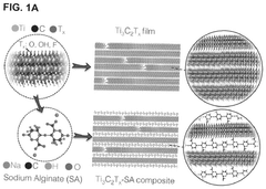
MXenes represent a revolutionary class of two-dimensional (2D) transition metal carbides, nitrides, and carbonitrides that were first discovered in 2011 by researchers at Drexel University. These materials are derived from MAX phases through selective etching of the A-layer atoms, resulting in a unique layered structure with exceptional electrical, optical, and mechanical properties. The general formula for MXenes is Mn+1XnTx, where M represents a transition metal, X is carbon or nitrogen, and Tx denotes surface terminations such as -OH, -O, or -F groups.
The evolution of MXenes has been marked by significant breakthroughs in synthesis methods and property characterization. Initially limited to a few compositions, the MXene family has expanded to include over 30 different compositions with various transition metals including titanium, molybdenum, niobium, and vanadium. This diversity has enabled tailored properties for specific applications, particularly in optoelectronic devices requiring transparent conductive films (TCFs).
The optoelectronics industry has long relied on indium tin oxide (ITO) as the standard material for transparent electrodes. However, ITO faces limitations including brittleness, scarcity of indium, and high processing temperatures. These challenges have driven the search for alternative TCF materials, positioning MXenes as promising candidates due to their unique combination of high electrical conductivity and optical transparency.
MXenes exhibit metallic conductivity with sheet resistances as low as 10 Ω/sq while maintaining optical transmittance above 90% in the visible spectrum for ultrathin films. Their solution processability enables cost-effective deposition methods including spray coating, spin coating, and inkjet printing, which are compatible with flexible substrates and large-area manufacturing.
The development goals for MXenes in transparent conductive film applications focus on several key aspects. First, enhancing the environmental stability of MXenes, as their surface-terminated structure makes them susceptible to oxidation in ambient conditions. Second, optimizing the trade-off between optical transparency and electrical conductivity through precise control of film thickness, composition, and surface chemistry. Third, developing scalable and reproducible synthesis methods that maintain consistent quality across large-area films.
Long-term technical objectives include achieving sheet resistance values below 50 Ω/sq with optical transmittance exceeding 90% in films stable for years under ambient conditions. Additionally, researchers aim to develop MXene-based TCFs compatible with emerging technologies such as flexible displays, wearable electronics, and perovskite solar cells, where traditional TCF materials face significant limitations.
The convergence of these development efforts positions MXenes as a transformative material platform for next-generation optoelectronic devices, potentially enabling advances in touchscreens, smart windows, organic light-emitting diodes, and photovoltaic cells with enhanced performance and novel functionalities.
Market Analysis for Transparent Conductive Films
The transparent conductive film (TCF) market is experiencing robust growth, driven by the expanding optoelectronics industry. Currently valued at approximately $5.1 billion in 2023, the TCF market is projected to reach $8.7 billion by 2028, representing a compound annual growth rate (CAGR) of 11.3%. This growth trajectory is primarily fueled by increasing demand for touchscreens, displays, photovoltaic cells, and emerging flexible electronics applications.
Indium Tin Oxide (ITO) continues to dominate the market with over 70% market share due to its established manufacturing ecosystem and reliable performance characteristics. However, ITO faces significant supply chain vulnerabilities due to indium's scarcity and geopolitical factors affecting its availability, creating a pressing need for alternative materials like MXenes.
The smartphone and tablet segment currently represents the largest application area for TCFs, accounting for approximately 45% of the total market. However, the fastest growth is observed in emerging sectors such as wearable devices (projected 18% CAGR) and flexible displays (projected 22% CAGR), where traditional ITO films face limitations due to their inherent brittleness.
Regional analysis reveals Asia-Pacific as the dominant market, controlling 65% of global TCF production, with China, South Korea, and Japan leading manufacturing capabilities. North America and Europe follow with 18% and 12% market shares respectively, focusing primarily on high-end applications and research advancements.
Consumer electronics manufacturers represent the largest end-user segment (58%), followed by solar industry applications (22%) and automotive displays (11%). The remaining market share is distributed among various emerging applications including smart windows, healthcare devices, and aerospace instrumentation.
Key market drivers include the growing adoption of OLED displays, increasing integration of touch interfaces across product categories, expanding solar energy installations, and the emergence of Internet of Things (IoT) devices requiring advanced display technologies. Additionally, sustainability concerns are creating market pull for environmentally friendly alternatives to traditional TCF materials.
Market challenges include price sensitivity in consumer electronics, technical performance requirements becoming increasingly stringent, and manufacturing scalability issues for novel materials like MXenes. Despite these challenges, the fundamental demand for higher-performing, flexible, and sustainable TCF solutions presents significant opportunities for MXene-based technologies to capture market share from established materials.
Current Status and Challenges of MXenes in Optoelectronics
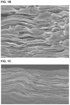
MXenes have emerged as promising materials for transparent conductive films (TCFs) in optoelectronic applications due to their unique combination of high electrical conductivity, optical transparency, and mechanical flexibility. Currently, MXenes are being extensively investigated for applications in touchscreens, displays, solar cells, and flexible electronics. The most widely studied MXene for TCF applications is Ti3C2Tx, which has demonstrated sheet resistances as low as 10 Ω/sq with optical transmittance exceeding 90% in the visible spectrum.
Despite these promising results, several significant challenges hinder the widespread adoption of MXenes in commercial optoelectronic devices. The primary challenge is the oxidative instability of MXenes in ambient conditions, which leads to degradation of electrical properties over time. Research has shown that Ti3C2Tx films can lose up to 70% of their conductivity within two weeks of air exposure, necessitating effective encapsulation strategies or chemical modifications to enhance stability.
Another critical challenge is the scalable production of high-quality MXene films with uniform thickness and minimal defects. Current synthesis methods, including vacuum filtration and spin coating, often result in films with inconsistent properties across larger areas, limiting their industrial applicability. The development of roll-to-roll compatible deposition techniques remains an active area of research but has not yet reached the maturity required for mass production.
The surface chemistry of MXenes presents both opportunities and challenges. While the terminal groups (Tx) can be tailored to optimize specific properties, precise control over these functionalities remains difficult. This variability affects the work function, conductivity, and interfacial properties of MXene films, impacting their performance in device architectures.
From a geographical perspective, research on MXene-based TCFs is concentrated primarily in the United States, China, and South Korea, with Drexel University, where MXenes were first discovered, maintaining leadership in fundamental research. Chinese institutions have made significant advances in large-scale synthesis and device integration, while South Korean research groups have focused on enhancing the stability and performance of MXene films.
The integration of MXenes with other materials to form hybrid structures represents both a challenge and a frontier for innovation. While composites of MXenes with graphene, conductive polymers, and metal nanowires have shown enhanced stability and performance, optimizing these interfaces without compromising transparency or conductivity requires further investigation.
Environmental concerns regarding the etching processes used in MXene synthesis, particularly those involving hydrofluoric acid, also present challenges for industrial adoption. Alternative, greener synthesis routes are being explored but often result in MXenes with inferior properties compared to those produced by conventional methods.
Current MXene-Based TCF Technical Solutions
01 MXene-based transparent conductive films
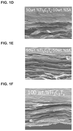
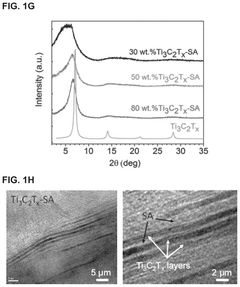
MXenes can be processed into transparent conductive films that combine high optical transparency with excellent electrical conductivity. These films are fabricated through methods such as solution processing, vacuum filtration, or spin coating to achieve uniform thin layers. The two-dimensional structure of MXenes allows for high electron mobility while maintaining optical transparency, making them suitable for applications in touchscreens, displays, and smart windows.- MXene-based transparent conductive films: MXenes can be processed into transparent conductive films that combine high optical transparency with excellent electrical conductivity. These films are fabricated through techniques such as solution processing, vacuum filtration, or spin coating to achieve uniform thin layers. The two-dimensional structure of MXenes allows for high electron mobility while maintaining optical transparency at appropriate thicknesses, making them suitable for applications in touchscreens, displays, and smart windows.
- Doping and surface modification of MXenes: The transparency and conductivity of MXenes can be enhanced through doping and surface modification techniques. By introducing specific elements or functional groups to the MXene surface, the electronic structure can be tuned to optimize both optical and electrical properties. Surface treatments can reduce defects, improve stability, and enhance charge carrier concentration, resulting in MXene materials with tailored transparency-conductivity relationships for specific applications.
- MXene-polymer composites for flexible transparent conductors: Combining MXenes with polymers creates flexible transparent conductive composites with enhanced mechanical properties. These composites maintain the high conductivity of MXenes while gaining flexibility and processability from the polymer matrix. The interaction between MXenes and polymers can be engineered to achieve optimal dispersion and interfacial bonding, resulting in composites with tunable transparency and conductivity suitable for flexible electronics, wearable devices, and stretchable displays.
- Thickness-dependent optical and electrical properties of MXenes: The transparency and conductivity of MXene films exhibit strong thickness dependence. As film thickness decreases, optical transparency increases while electrical conductivity may decrease due to quantum confinement effects and increased influence of surface scattering. Understanding and controlling this relationship is crucial for optimizing MXene films for specific applications. Various deposition and exfoliation techniques can be employed to precisely control film thickness and achieve the desired balance between transparency and conductivity.
- MXene-based hybrid materials with other 2D materials: Hybrid structures combining MXenes with other two-dimensional materials such as graphene, transition metal dichalcogenides, or metal oxides can exhibit synergistic effects on transparency and conductivity. These heterostructures leverage the complementary properties of different 2D materials to overcome individual limitations. Layer-by-layer assembly or in-situ growth methods can be used to create these hybrid materials with enhanced performance for applications in optoelectronics, photovoltaics, and transparent electrodes.
02 Tuning transparency and conductivity through composition control
The transparency and conductivity of MXene materials can be precisely tuned by controlling their composition, including the selection of transition metals (Ti, Mo, V, etc.) and surface termination groups (-O, -F, -OH). By adjusting these parameters, researchers can optimize the balance between optical transparency and electrical conductivity for specific applications. Surface functionalization can also be employed to enhance these properties while maintaining the 2D structure of MXenes.Expand Specific Solutions03 MXene-polymer composites for flexible transparent conductors
Incorporating MXenes into polymer matrices creates flexible transparent conductive composites with enhanced mechanical properties. These composites maintain the high conductivity of MXenes while gaining flexibility and durability from the polymer component. The resulting materials can be used in flexible electronics, wearable devices, and bendable displays where traditional rigid transparent conductors like ITO (indium tin oxide) are unsuitable. The polymer matrix also helps to prevent MXene sheet restacking, preserving their unique properties.Expand Specific Solutions04 Thickness-dependent optical and electrical properties
The transparency and conductivity of MXene films exhibit strong thickness dependence, allowing for application-specific optimization. Ultrathin MXene films (few nanometers) demonstrate high optical transparency with moderate conductivity, while thicker films show increased conductivity at the expense of reduced transparency. This relationship enables the design of MXene-based materials with precisely tailored optoelectronic properties for applications ranging from transparent electrodes to electromagnetic interference shielding.Expand Specific Solutions05 MXene hybrids with other 2D materials
Hybrid structures combining MXenes with other two-dimensional materials such as graphene, transition metal dichalcogenides, or metal oxides can achieve synergistic improvements in both transparency and conductivity. These heterostructures leverage the complementary properties of different 2D materials to overcome individual limitations. For example, MXene-graphene hybrids can exhibit enhanced conductivity while maintaining good transparency, and MXene-metal oxide combinations can provide improved stability while preserving the desired optoelectronic properties.Expand Specific Solutions
Key Industry Players in MXenes Research and Applications
The MXenes for transparent conductive films market is in an early growth phase, characterized by rapid technological advancement and expanding applications in optoelectronics. The global market size is projected to grow significantly as these materials offer superior conductivity and optical transparency compared to traditional alternatives. Technologically, research institutions like Drexel University (the pioneer in MXene discovery) and KAIST lead fundamental development, while companies including Murata Manufacturing, Nitto Denko, and Advanced Nano Products are advancing commercial applications. Chinese universities (Zhejiang, Fudan, Hunan) are rapidly closing the technology gap with significant research output. The ecosystem shows a balanced collaboration between academic institutions developing core technologies and industrial players focusing on scalable manufacturing processes and practical applications in displays, touch panels, and solar cells.
Drexel University
Technical Solution: Drexel University stands as the pioneering institution in MXene research, having first discovered and synthesized this class of 2D materials in 2011. Their approach to MXene-based transparent conductive films (TCFs) involves selective etching of MAX phases to produce Ti3C2Tx MXene nanosheets with controlled thickness and lateral dimensions. Drexel's technique employs vacuum-assisted filtration followed by delamination to create highly conductive, flexible, and transparent films. Their MXene TCFs demonstrate sheet resistances as low as 10 Ω/sq at 90% transparency, outperforming many conventional TCF materials. Drexel has developed scalable spray-coating and spin-coating methods for uniform MXene deposition on various substrates, enabling integration into optoelectronic devices including touchscreens, solar cells, and OLEDs. Their solution-processable MXene inks maintain excellent conductivity while achieving optical transmittance above 95% for ultrathin films.
Strengths: Pioneering expertise in MXene synthesis and processing; exceptional conductivity-transparency balance; solution-processability enabling various deposition techniques; strong intellectual property portfolio. Weaknesses: Challenges in long-term environmental stability of MXene films; oxidation susceptibility in ambient conditions; relatively high production costs compared to established TCF materials.
Korea Advanced Institute of Science & Technology
Technical Solution: KAIST has developed innovative approaches to MXene-based transparent conductive films focusing on enhanced stability and optoelectronic performance. Their technology utilizes a controlled oxidation strategy that creates partially oxidized MXene films with improved environmental stability while maintaining high conductivity. KAIST researchers have pioneered hybrid structures combining MXenes with other nanomaterials like graphene and silver nanowires, creating synergistic composites with optimized transparency and conductivity. Their spray-coated Ti3C2Tx MXene films achieve sheet resistance of approximately 8.8 Ω/sq at 91% transparency, among the highest performance metrics reported. KAIST has also developed novel surface functionalization techniques that enhance MXene film adhesion to various substrates while improving resistance to oxidative degradation. Their MXene TCFs have been successfully integrated into flexible displays, touch panels, and photovoltaic devices with demonstrated durability under repeated mechanical deformation.
Strengths: Advanced hybrid material engineering; excellent conductivity-transparency trade-off; enhanced environmental stability through surface modifications; demonstrated integration in commercial-relevant devices. Weaknesses: Complex multi-step fabrication processes may limit mass production; higher material costs compared to conventional ITO; requires specialized equipment for optimal film deposition.
Critical Patents and Innovations in MXene TCF Technology
Two-dimensional metal carbide, nitride, and carbonitride films and composites for EMI shielding
PatentWO2017184957A1
Innovation
- The use of two-dimensional (2D) transition metal carbides, nitrides, and carbonitrides, specifically MXene films and MXene-polymer composites, which provide high EMI shielding effectiveness due to their exceptional electrical conductivity and mechanical properties, outperforming traditional materials by offering lightweight, flexible, and easily fabricated solutions.

Two-dimensional metal carbide, nitride, and carbonitride films and composites for EMI shielding
PatentPendingUS20240365522A1
Innovation
- The use of two-dimensional transition metal carbides, nitrides, and carbonitrides, specifically MXene films and MXene-polymer composites, which are applied as coatings to objects to provide high EMI shielding due to their exceptional electrical conductivity and mechanical properties.
Manufacturing Scalability and Cost Analysis
The scalability of MXene manufacturing processes represents a critical factor in determining their commercial viability for transparent conductive films in optoelectronics. Current laboratory-scale synthesis methods predominantly rely on selective etching of MAX phases using hydrofluoric acid (HF), followed by delamination processes. While these methods produce high-quality MXene flakes, they face significant challenges when scaled to industrial production levels.
Production scaling requires substantial capital investment in specialized equipment for handling hazardous chemicals and maintaining precise process control. The transition from batch processing to continuous flow manufacturing remains technically challenging, with current throughput limitations of approximately 10-50 grams per batch in optimized laboratory settings. Industrial requirements for optoelectronic applications would necessitate kilogram to ton-scale production capabilities.
Cost analysis reveals that raw material expenses constitute approximately 30-40% of total production costs, with MAX phase precursors and etching agents being the primary contributors. Labor and energy costs account for another 25-30%, while equipment depreciation and maintenance represent 15-20%. The estimated production cost currently ranges from $2,000-5,000 per kilogram of high-quality MXene, significantly higher than established transparent conductor materials like ITO ($700-900/kg).
Several promising approaches for cost reduction and scalability improvement have emerged. These include the development of HF-free etching methods using Lewis acid molten salts, which could reduce hazardous waste management costs by 40-60%. Continuous flow reactors show potential to increase throughput by 5-10 times while maintaining quality consistency. Additionally, recycling of etching solutions could decrease chemical costs by 20-30%.
Market analysis suggests that MXene production costs must decrease to below $1,000 per kilogram to achieve competitive positioning against established transparent conductive materials. This price point appears achievable within 3-5 years through process optimization and economies of scale, particularly if annual production volumes exceed 100 kilograms.
The environmental impact of manufacturing processes presents both challenges and opportunities. While current methods generate significant hazardous waste, emerging green synthesis approaches could potentially position MXenes as environmentally advantageous alternatives to rare-earth-containing transparent conductors, potentially offsetting higher production costs through regulatory advantages and sustainability marketing.
Environmental Impact and Sustainability Considerations
The environmental footprint of MXenes in transparent conductive film applications represents a critical consideration for sustainable optoelectronic development. MXene synthesis typically involves etching processes using hydrofluoric acid or fluoride salts, which pose significant environmental and health hazards if not properly managed. These processes generate acidic waste streams containing metal ions and fluoride compounds that require specialized treatment protocols to prevent environmental contamination. However, recent advancements have introduced greener synthesis routes utilizing milder etchants and environmentally benign solvents, substantially reducing the ecological impact of production.
When compared to traditional transparent conductive materials like indium tin oxide (ITO), MXenes offer notable sustainability advantages. The scarcity of indium has raised concerns about ITO's long-term viability, whereas MXenes utilize more abundant transition metals such as titanium, molybdenum, and niobium. This shift toward more plentiful resources alleviates supply chain vulnerabilities and reduces the environmental degradation associated with rare metal mining operations.
The energy consumption profile of MXene-based devices presents another dimension of environmental consideration. Preliminary life cycle assessments indicate that MXene films can be processed at lower temperatures than conventional alternatives, potentially reducing the carbon footprint of manufacturing processes. Additionally, the exceptional electrical properties of MXenes may contribute to improved energy efficiency in final optoelectronic applications, including solar cells and energy-efficient displays, thereby offsetting initial production impacts through operational benefits.
End-of-life management for MXene-containing devices remains an underdeveloped area requiring further research. Current electronic waste recycling systems are not optimized for recovering nanomaterials like MXenes, potentially leading to material loss and environmental release. Developing closed-loop recycling methodologies specifically designed for MXene recovery could significantly enhance the sustainability profile of these materials.
Water usage during MXene production and processing represents another environmental concern. The colloidal processing of MXenes typically involves substantial water consumption, though recent innovations in solvent recycling and waterless deposition techniques show promise for reducing this impact. Implementation of these advanced processing methods could substantially decrease the water footprint associated with MXene-based transparent conductive films.
Regulatory frameworks governing nanomaterial production and disposal are evolving globally, with increasing emphasis on environmental protection and sustainable practices. Manufacturers incorporating MXenes into optoelectronic devices must navigate these emerging regulations while implementing robust environmental management systems that address the unique challenges posed by these advanced materials throughout their lifecycle.
Unlock deeper insights with Patsnap Eureka Quick Research — get a full tech report to explore trends and direct your research. Try now!
Generate Your Research Report Instantly with AI Agent
Supercharge your innovation with Patsnap Eureka AI Agent Platform!