Ammonium hydroxide as an etchant in microelectronics
AUG 14, 20259 MIN READ
Generate Your Research Report Instantly with AI Agent
PatSnap Eureka helps you evaluate technical feasibility & market potential.
Ammonium Hydroxide Etching Background and Objectives
Ammonium hydroxide has emerged as a crucial etchant in the microelectronics industry, playing a significant role in the fabrication of semiconductor devices. The evolution of this technology can be traced back to the early days of integrated circuit manufacturing, where wet etching processes were predominant. As the demand for smaller and more complex electronic components grew, the need for precise and controllable etching techniques became paramount.
The use of ammonium hydroxide as an etchant gained traction due to its unique properties and compatibility with various materials used in microelectronics. Its ability to selectively etch certain materials while leaving others intact has made it an invaluable tool in the semiconductor industry. The development of ammonium hydroxide etching techniques has been closely tied to the advancement of photolithography and other microfabrication processes.
Over the years, researchers and engineers have continuously refined the application of ammonium hydroxide in etching processes, focusing on improving etch rates, selectivity, and uniformity. The technology has evolved from simple immersion etching to more sophisticated methods, including spray etching and vapor phase etching, each offering specific advantages for different applications.
The primary objective of research in ammonium hydroxide etching is to enhance its effectiveness and precision in microelectronics manufacturing. This includes developing optimized etching recipes for various materials, improving etch uniformity across large wafers, and minimizing unwanted side effects such as undercut or surface roughness. Additionally, there is a strong focus on understanding the fundamental mechanisms of the etching process at the atomic level.
Another key goal is to integrate ammonium hydroxide etching into advanced manufacturing processes, such as those used for 3D integrated circuits and next-generation semiconductor devices. This involves addressing challenges related to compatibility with other fabrication steps, scalability, and environmental considerations.
As the microelectronics industry continues to push the boundaries of device miniaturization and performance, the role of ammonium hydroxide etching becomes increasingly critical. Future research aims to explore novel applications of this technology, including its potential use in emerging fields like quantum computing and flexible electronics. The ongoing development of ammonium hydroxide etching techniques is expected to contribute significantly to the advancement of microelectronics technology, enabling the creation of more sophisticated and efficient electronic devices.
Market Demand Analysis for Microelectronics Etching
The market demand for microelectronics etching solutions, particularly those involving ammonium hydroxide as an etchant, has been steadily growing in recent years. This growth is primarily driven by the continuous miniaturization of electronic devices and the increasing complexity of integrated circuits. The global semiconductor industry, which heavily relies on etching processes, is projected to reach a market value of over $600 billion by 2025, indicating a substantial demand for advanced etching technologies.
Ammonium hydroxide-based etching solutions have gained significant attention in the microelectronics industry due to their unique properties and advantages over traditional etchants. These solutions offer improved selectivity, better control over etching rates, and reduced environmental impact compared to conventional acid-based etchants. As a result, the market for ammonium hydroxide etching solutions is expected to grow at a compound annual growth rate (CAGR) of around 6% from 2021 to 2026.
The demand for ammonium hydroxide as an etchant is particularly strong in the production of advanced logic and memory chips, where precise control over feature sizes and shapes is critical. With the increasing adoption of 7nm, 5nm, and even 3nm process nodes in semiconductor manufacturing, the need for highly selective and controllable etching solutions has become more pronounced. This trend is expected to continue as the industry moves towards even smaller process nodes and more complex 3D chip architectures.
In addition to the semiconductor industry, the market for ammonium hydroxide etching solutions is also expanding in other microelectronics sectors, such as MEMS (Micro-Electro-Mechanical Systems) and photonics. These emerging applications require specialized etching processes that can achieve high aspect ratios and smooth surfaces, further driving the demand for advanced etching technologies.
The Asia-Pacific region, particularly countries like Taiwan, South Korea, and China, dominates the market for microelectronics etching solutions. This is due to the concentration of semiconductor manufacturing facilities in these countries. However, there is also growing demand in North America and Europe, driven by investments in domestic semiconductor production and research into next-generation technologies.
Environmental regulations and sustainability concerns are also shaping the market demand for etching solutions. Ammonium hydroxide-based etchants are gaining favor due to their lower environmental impact compared to traditional acid-based solutions. This aligns with the industry's push towards more sustainable manufacturing processes and has led to increased research and development efforts in this area.
Current State and Challenges of Ammonium Hydroxide Etching
Ammonium hydroxide etching has become a crucial process in microelectronics manufacturing, particularly in the fabrication of semiconductor devices. The current state of this technology is characterized by its widespread adoption in various applications, including silicon wafer cleaning, photoresist stripping, and metal etching. The effectiveness of ammonium hydroxide as an etchant lies in its ability to remove organic contaminants and certain metal impurities from semiconductor surfaces.
In recent years, significant advancements have been made in optimizing the etching process using ammonium hydroxide. Researchers have developed precise control mechanisms for etch rates and selectivity, allowing for more accurate and uniform etching across wafer surfaces. Additionally, the integration of ammonium hydroxide etching into advanced cleaning processes, such as the RCA clean, has further enhanced its importance in the semiconductor industry.
Despite these advancements, several challenges persist in the use of ammonium hydroxide as an etchant. One of the primary concerns is the potential for surface roughening, especially when used at high concentrations or for extended periods. This can lead to degradation of device performance and yield issues in subsequent manufacturing steps. Furthermore, the etching process can be sensitive to temperature variations, requiring precise control to maintain consistent results.
Another significant challenge is the environmental impact of ammonium hydroxide usage. As the semiconductor industry faces increasing pressure to adopt more sustainable practices, there is a growing need to develop eco-friendly alternatives or to implement more efficient recycling and waste management systems for ammonium hydroxide-based etchants.
The industry is also grappling with the limitations of ammonium hydroxide etching in advanced node technologies. As device dimensions continue to shrink, there is a demand for even more precise and controlled etching processes. This has led to research into alternative etchants and hybrid etching techniques that can offer better selectivity and less damage to delicate nanostructures.
From a geographical perspective, the development and implementation of ammonium hydroxide etching technologies are primarily concentrated in regions with strong semiconductor manufacturing bases, such as East Asia, North America, and Europe. These areas continue to drive innovation in etching processes, with a focus on addressing the current challenges and pushing the boundaries of what is possible with ammonium hydroxide-based etching.
In conclusion, while ammonium hydroxide etching remains a critical technology in microelectronics manufacturing, it faces several challenges that require ongoing research and development. The industry is actively working to overcome these obstacles, with a focus on improving process control, reducing environmental impact, and adapting the technology to meet the demands of next-generation semiconductor devices.
Existing Ammonium Hydroxide Etching Solutions
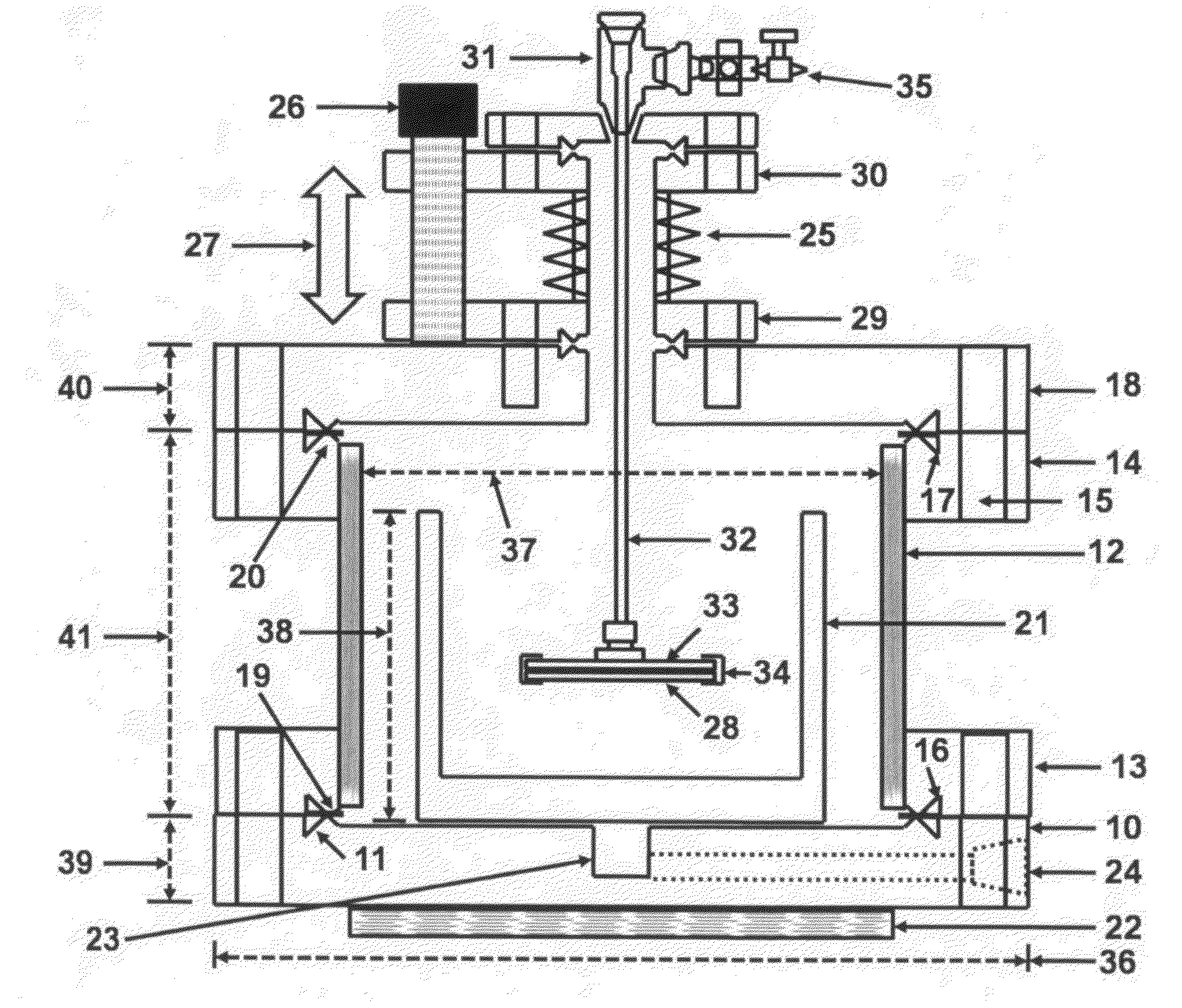
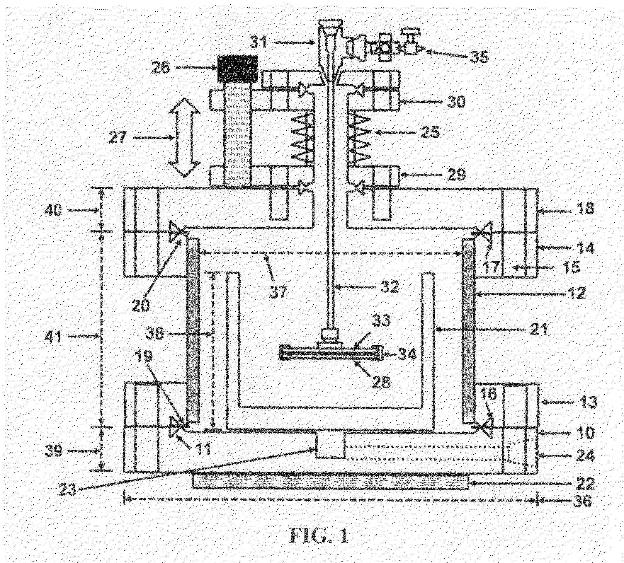
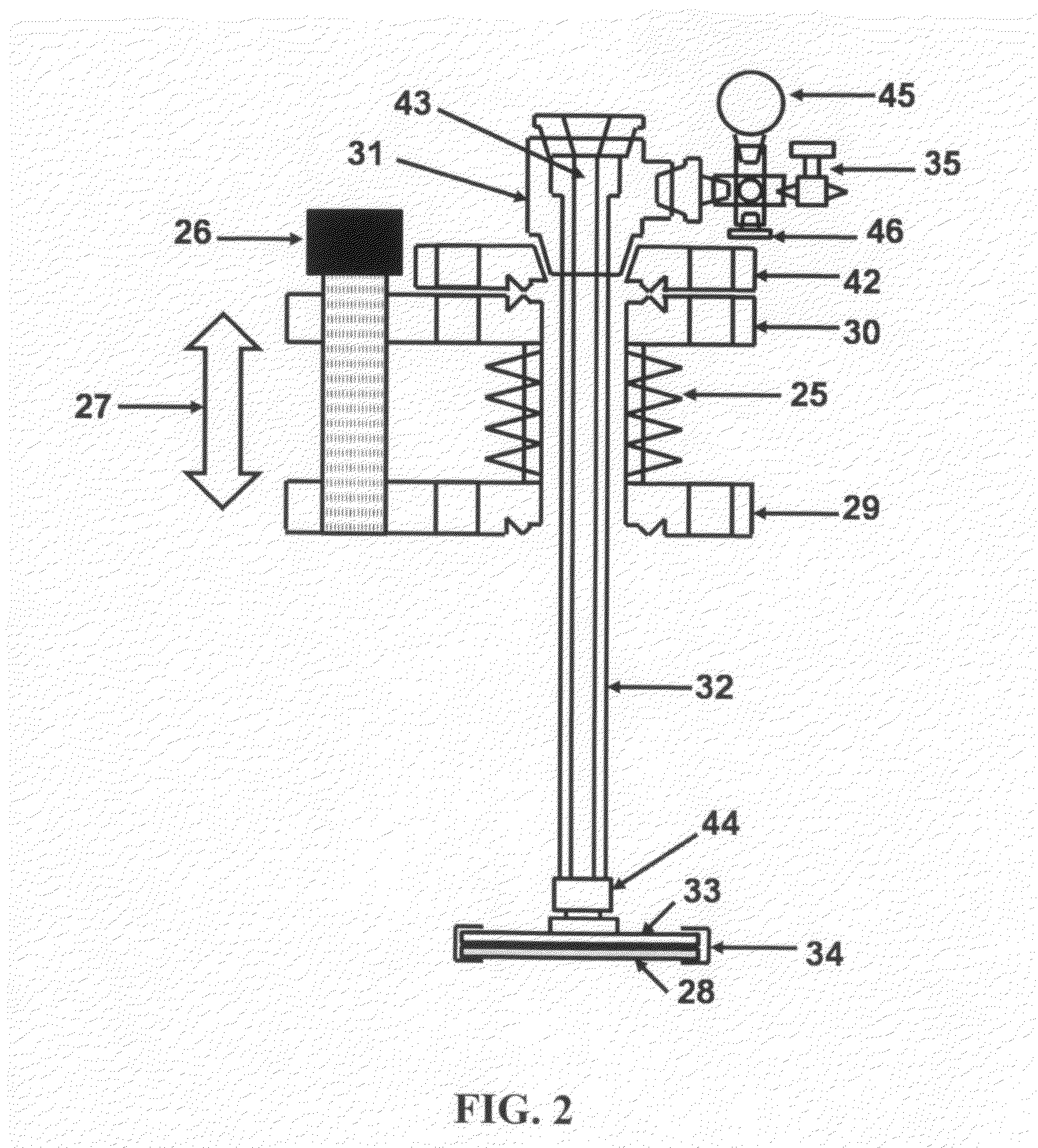
01 Etching of semiconductor materials
Ammonium hydroxide is used in etching processes for semiconductor materials, particularly in the fabrication of integrated circuits. The etching solution often includes a mixture of ammonium hydroxide with other chemicals like hydrogen peroxide and water, known as the RCA clean. This process helps remove contaminants and create desired surface structures on silicon wafers.- Etching of semiconductor materials: Ammonium hydroxide is used in etching processes for semiconductor materials, particularly in the fabrication of integrated circuits. The etching solution often includes a mixture of ammonium hydroxide with other chemicals like hydrogen peroxide and water, known as the RCA clean. This process helps remove contaminants and create desired surface structures on silicon wafers.
- Metal etching applications: Ammonium hydroxide is utilized in etching various metals and metal alloys. It can be used alone or in combination with other chemicals to selectively remove metal layers or create specific patterns on metal surfaces. This technique is applied in industries such as electronics manufacturing and metalworking.
- Glass and ceramic etching: Ammonium hydroxide plays a role in etching glass and ceramic materials. It can be used to modify surface properties, create patterns, or remove unwanted layers. This process is relevant in the production of optical components, decorative glassware, and certain electronic devices.
- Etching in printed circuit board manufacturing: In the production of printed circuit boards (PCBs), ammonium hydroxide etching is employed to create conductive patterns on copper-clad laminates. The process involves selectively removing copper from areas not protected by a resist, leaving behind the desired circuit pattern.
- Environmental and safety considerations in etching processes: The use of ammonium hydroxide in etching processes requires careful consideration of environmental and safety factors. This includes proper handling, storage, and disposal of etching solutions, as well as implementing measures to control emissions and protect workers from exposure. Developments in this area focus on improving process efficiency while minimizing environmental impact.
02 Metal etching applications
Ammonium hydroxide is utilized in etching various metals and metal alloys. It can be used alone or in combination with other chemicals to selectively remove metal layers or create specific patterns on metal surfaces. This technique is applied in industries such as electronics manufacturing and metalworking.Expand Specific Solutions03 Etching of glass and ceramics
Ammonium hydroxide etching is employed in the processing of glass and ceramic materials. It can be used to modify surface properties, create textures, or remove unwanted layers. This technique finds applications in the production of optical components, decorative glassware, and advanced ceramic materials.Expand Specific Solutions04 Controlled etching in nanomaterial fabrication
Ammonium hydroxide etching plays a role in the fabrication and modification of nanomaterials. It can be used to control the size, shape, and surface properties of nanoparticles and nanostructures. This technique is particularly useful in creating advanced materials for applications in electronics, energy storage, and catalysis.Expand Specific Solutions05 Environmental and safety considerations
The use of ammonium hydroxide in etching processes requires careful consideration of environmental and safety factors. Proper handling, storage, and disposal procedures must be implemented to minimize risks to workers and the environment. Additionally, research is ongoing to develop more environmentally friendly etching alternatives or to optimize existing processes to reduce the use of hazardous chemicals.Expand Specific Solutions
Key Players in Microelectronics Etching Industry
The research on ammonium hydroxide as an etchant in microelectronics is in a mature stage, with a competitive landscape shaped by established players and ongoing innovation. The market for this technology is substantial, driven by the growing demand for advanced semiconductor manufacturing processes. Key players like Samsung Electronics, Texas Instruments, and GlobalFoundries are actively involved in developing and refining etching techniques. The technology's maturity is evident in its widespread adoption across the industry, with companies such as FUJIFILM Electronic Materials and Tokyo Ohka Kogyo providing specialized chemical solutions. However, there is still room for improvement and optimization, particularly in areas of selectivity, uniformity, and environmental impact.
Samsung Electronics Co., Ltd.
Technical Solution: Samsung Electronics has developed an advanced ammonium hydroxide-based etching process for microelectronics fabrication. Their technique utilizes a precisely controlled NH4OH solution concentration, typically ranging from 0.5% to 5%, to achieve highly selective etching of silicon dioxide and silicon nitride layers[1]. The company has implemented this process in their state-of-the-art 5nm and 3nm node semiconductor manufacturing, allowing for the creation of ultra-fine features and high-aspect-ratio structures[2]. Samsung's method also incorporates a unique post-etch treatment using dilute hydrofluoric acid to remove any residual oxide, resulting in improved surface smoothness and reduced defect density[3].
Strengths: Precise control over etching selectivity, compatibility with advanced node processes, and improved surface quality. Weaknesses: Potential for ammonia gas evolution requiring stringent safety measures, and the need for specialized equipment for handling corrosive chemicals.
Semiconductor Manufacturing International (Shanghai) Corp.
Technical Solution: SMIC has developed a proprietary ammonium hydroxide-based etching solution for use in their advanced semiconductor manufacturing processes. Their approach combines NH4OH with hydrogen peroxide and deionized water in a specific ratio, known as the SC-1 (Standard Clean-1) solution[4]. This mixture is used in a multi-step cleaning and etching process, where the ammonium hydroxide component plays a crucial role in removing organic contaminants and etching silicon surfaces. SMIC has optimized this process for their 14nm and 28nm technology nodes, achieving etch rates of approximately 0.7-1.2 nm/min for silicon dioxide layers[5]. The company has also implemented an in-situ monitoring system to ensure precise control over the etching process, maintaining consistent feature sizes and reducing variability in device performance[6].
Strengths: Effective removal of organic contaminants, controllable etch rates, and integration with existing cleaning processes. Weaknesses: Limited selectivity compared to more advanced etching techniques, and potential for surface roughening if not carefully controlled.
Core Innovations in Ammonium Hydroxide Etching
Hafnium oxide corrosion inhibitor
PatentActiveUS11946148B2
Innovation
- An aqueous etching solution comprising water, alkaline ammonium compounds, peroxide compounds, water-miscible organic solvents, nitrogen-containing compounds, and optionally chelating agents, which provides selective etching of TiSiN over HfO2 with an etch selectivity greater than 30, ensuring preferential removal of TiSiN without harming the HfO2 layer.


High purity, environmentally clean method and apparatus, for high rate, liquid anisotropic etching of single crystal silicon or etching of polycrystalline silicon, using an overpressure of ammonia gas above aqueous ammonium hydroxide
PatentInactiveUS20130012028A1
Innovation
- The use of high purity aqueous ammonium hydroxide (NH4OH) solution generated at the point of use from semiconductor grade ammonia gas dissolved in deionized water, maintained in a hermetically enclosed chamber with an overpressure of ammonia, preventing evaporation and allowing high anisotropic etching rates at temperatures between 70-90°C.

Environmental Impact of Ammonium Hydroxide Etching
The use of ammonium hydroxide as an etchant in microelectronics has significant environmental implications that warrant careful consideration. While effective for certain etching processes, ammonium hydroxide poses potential risks to both human health and the environment if not properly managed.
One of the primary environmental concerns is the release of ammonia gas during the etching process. Ammonia is a potent air pollutant that can contribute to the formation of particulate matter and smog. When released into the atmosphere, it can react with other compounds to form fine particles that negatively impact air quality and human respiratory health. Additionally, ammonia emissions can lead to eutrophication of water bodies, causing algal blooms and disrupting aquatic ecosystems.
The disposal of spent ammonium hydroxide solutions presents another environmental challenge. If not properly treated, these waste streams can contaminate soil and water resources. The high pH of ammonium hydroxide solutions can alter the chemistry of receiving water bodies, potentially harming aquatic life. Furthermore, the nitrogen content in these solutions can contribute to nutrient pollution, exacerbating issues of eutrophication in freshwater and marine environments.
From a resource perspective, the production of ammonium hydroxide requires energy and raw materials, contributing to the overall environmental footprint of microelectronics manufacturing. The Haber-Bosch process, used to synthesize ammonia, is energy-intensive and typically relies on fossil fuels, leading to greenhouse gas emissions and resource depletion.
To mitigate these environmental impacts, the microelectronics industry has been exploring various strategies. These include implementing closed-loop recycling systems for ammonium hydroxide, developing more efficient etching processes to reduce chemical consumption, and investigating alternative etchants with lower environmental impact. Advanced wastewater treatment technologies are also being employed to neutralize and remove ammonia from effluents before discharge.
Regulatory frameworks play a crucial role in managing the environmental risks associated with ammonium hydroxide use. Many jurisdictions have implemented strict guidelines for the handling, storage, and disposal of this chemical, as well as emission controls to limit atmospheric releases. Compliance with these regulations is essential for microelectronics manufacturers to minimize their environmental footprint and ensure sustainable operations.
As the industry continues to evolve, there is a growing emphasis on green chemistry principles and the development of more environmentally benign etching processes. Research into bio-based etchants and electrochemical etching techniques shows promise for reducing the reliance on harsh chemicals like ammonium hydroxide. These advancements not only address environmental concerns but also align with broader sustainability goals in the microelectronics sector.
Safety Protocols in Ammonium Hydroxide Etching
Safety protocols in ammonium hydroxide etching are critical for ensuring the well-being of personnel and maintaining a secure working environment in microelectronics manufacturing. The use of ammonium hydroxide as an etchant requires stringent safety measures due to its corrosive and potentially harmful nature.
Personal protective equipment (PPE) is paramount when handling ammonium hydroxide. Workers must wear chemical-resistant gloves, safety goggles, face shields, and appropriate protective clothing. Respiratory protection may also be necessary, especially in areas with inadequate ventilation.
Proper ventilation systems are essential to minimize exposure to ammonia vapors. Fume hoods or local exhaust ventilation should be utilized during etching processes to remove harmful fumes and maintain air quality within acceptable limits. Regular maintenance and testing of these systems are crucial to ensure their effectiveness.
Emergency response procedures must be clearly defined and communicated to all personnel. This includes the location and proper use of eyewash stations, safety showers, and spill containment equipment. Regular drills should be conducted to familiarize staff with emergency protocols and evacuation procedures.
Storage and handling of ammonium hydroxide require specific safety measures. The chemical should be stored in a cool, well-ventilated area, away from incompatible materials. Proper labeling and secondary containment are necessary to prevent accidental spills and minimize risks associated with storage.
Training programs are vital to ensure all personnel understand the hazards associated with ammonium hydroxide and the proper safety procedures. This includes instruction on the correct use of PPE, handling techniques, emergency response, and the importance of following established protocols.
Regular safety audits and inspections should be conducted to identify potential hazards and ensure compliance with safety standards. This includes checking the integrity of storage containers, verifying the functionality of safety equipment, and assessing the overall safety culture within the facility.
Waste management is another crucial aspect of safety protocols. Proper disposal methods for spent etchant solutions and contaminated materials must be implemented to prevent environmental contamination and comply with regulatory requirements.
By implementing comprehensive safety protocols, microelectronics manufacturers can significantly reduce the risks associated with ammonium hydroxide etching, protecting their workforce and maintaining a safe and productive working environment.
Unlock deeper insights with PatSnap Eureka Quick Research — get a full tech report to explore trends and direct your research. Try now!
Generate Your Research Report Instantly with AI Agent
Supercharge your innovation with PatSnap Eureka AI Agent Platform!