

Why 2D Semiconductors Transform Electronics Industry
OCT 14, 20259 MIN READ
Generate Your Research Report Instantly with AI Agent
PatSnap Eureka helps you evaluate technical feasibility & market potential.
2D Semiconductor Evolution and Research Objectives
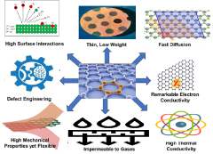
Two-dimensional (2D) semiconductors represent a revolutionary class of materials that have emerged from the broader family of 2D materials, first pioneered by the isolation of graphene in 2004. Unlike traditional three-dimensional semiconductors, these atomically thin materials exhibit unique electronic, optical, and mechanical properties that arise from quantum confinement effects when electrons are restricted to movement in a plane.
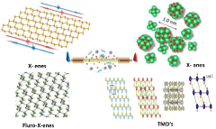
The evolution of 2D semiconductor technology can be traced through several distinct phases. The initial discovery phase (2004-2010) focused primarily on graphene, which despite its remarkable properties, lacks a natural bandgap—a critical requirement for semiconductor applications. This limitation prompted researchers to explore other 2D materials, leading to the exploration phase (2010-2015) that witnessed the emergence of transition metal dichalcogenides (TMDs) such as MoS2, WS2, and WSe2, which naturally possess suitable bandgaps.
The characterization phase (2015-2020) involved intensive efforts to understand the fundamental properties of these materials, including their band structures, carrier mobilities, and quantum behaviors. This period saw significant advancements in fabrication techniques, enabling the production of higher quality samples with fewer defects and impurities.
Currently, we are in the application development phase (2020-present), where research is increasingly focused on integrating 2D semiconductors into practical devices and exploring their potential in various technological domains. This includes flexible electronics, ultra-efficient photovoltaics, and quantum computing components.
The primary research objectives in this field are multifaceted. First, there is a pressing need to develop scalable and reproducible fabrication methods that can transition 2D semiconductors from laboratory curiosities to industrial-scale production. This includes addressing challenges in large-area synthesis, layer control, and interface engineering.
Second, researchers aim to enhance the electronic performance of these materials through strategies such as strain engineering, defect management, and heterostructure formation—where different 2D materials are stacked to create novel electronic properties.
Third, there is significant interest in exploring the unique quantum phenomena exhibited by 2D semiconductors, including valley polarization, exciton dynamics, and topological states, which could enable entirely new classes of electronic and photonic devices.
Finally, the ultimate objective is to demonstrate practical applications that leverage the distinctive advantages of 2D semiconductors—such as ultimate thinness, flexibility, transparency, and unique electronic properties—to create electronic systems that outperform conventional technologies in specific niches or enable entirely new functionalities previously unattainable.
Market Potential and Industry Applications
The 2D semiconductor market is experiencing unprecedented growth, with projections indicating a compound annual growth rate exceeding 20% through 2030. This remarkable expansion is driven by the unique properties of 2D materials that enable applications impossible with traditional silicon technology. The global market value, currently estimated at several hundred million dollars, is expected to reach multiple billions within the decade as commercialization accelerates.
Consumer electronics represents the most immediate and substantial market opportunity. Major smartphone manufacturers are actively researching 2D semiconductor integration for next-generation devices, particularly focusing on flexible displays, ultra-efficient processors, and extended battery life. The wearable technology segment shows particular promise, with 2D materials enabling truly flexible, conformable electronics that can be integrated into clothing, accessories, and even directly onto skin.
In the automotive sector, 2D semiconductors are positioned to revolutionize both conventional and electric vehicles. Their superior thermal management capabilities address critical challenges in power electronics, while their sensing properties enable advanced driver assistance systems. Several major automotive manufacturers have established dedicated research divisions focused exclusively on 2D material integration for next-generation vehicles.
The healthcare and biomedical industries represent another significant growth vector. The biocompatibility and sensing capabilities of certain 2D materials make them ideal for implantable medical devices, continuous health monitoring systems, and point-of-care diagnostics. Early clinical trials of biosensors utilizing 2D materials have demonstrated sensitivity levels orders of magnitude greater than conventional technologies.
Aerospace and defense applications leverage the extreme durability and radiation resistance of 2D semiconductors. These properties make them particularly valuable for satellite communications, space exploration equipment, and military electronics operating in harsh environments. Several space agencies have already deployed experimental systems incorporating 2D materials in low-earth orbit.
The energy sector is exploring 2D semiconductors for next-generation solar cells, energy storage solutions, and smart grid technologies. Laboratory prototypes have demonstrated theoretical efficiency improvements of 15-30% compared to current technologies, though commercial-scale production remains challenging.
Industrial applications include advanced sensors for manufacturing environments, where the extreme sensitivity and stability of 2D materials enable more precise process control and predictive maintenance. Early adopters in semiconductor manufacturing, pharmaceutical production, and chemical processing report significant improvements in quality control and operational efficiency.
Technical Barriers and Global Development Status
Despite the promising potential of 2D semiconductors, several significant technical barriers impede their widespread adoption in the electronics industry. The primary challenge lies in the scalable production of high-quality, defect-free 2D materials. Current synthesis methods, including mechanical exfoliation and chemical vapor deposition (CVD), struggle to produce large-area, uniform films with consistent properties at industrial scales. This manufacturing inconsistency creates substantial yield issues that prevent mass production.
Contact resistance represents another critical barrier, as the interface between 2D materials and metal contacts often exhibits high resistance, degrading device performance. Engineers have yet to develop reliable methods for creating low-resistance contacts that maintain the intrinsic properties of 2D semiconductors while enabling efficient charge transport.
Stability and encapsulation challenges persist, with many 2D materials showing sensitivity to environmental factors such as oxygen and moisture. This vulnerability necessitates sophisticated encapsulation techniques that add complexity to device fabrication while potentially compromising performance advantages.
The global development landscape for 2D semiconductors shows distinct regional specialization. The United States leads in fundamental research and intellectual property, with institutions like MIT, Stanford, and companies such as IBM making significant contributions to the theoretical understanding and early applications of these materials. The National Science Foundation has established dedicated centers for 2D materials research, fostering collaboration between academia and industry.
Asia, particularly South Korea and China, has emerged as a powerhouse in manufacturing-oriented research. Samsung and TSMC have made substantial investments in 2D semiconductor integration with existing silicon technologies. China's rapid advancement is evident through increased patent filings and government-backed initiatives focusing on commercial applications of graphene and other 2D materials.
Europe maintains strength in materials science innovation, with the Graphene Flagship program representing the EU's €1 billion commitment to transitioning graphene and related materials from research laboratories to commercial applications. The UK, Germany, and France host specialized research centers developing novel synthesis methods and device architectures.
The development status varies significantly across different 2D materials. Graphene has reached commercial viability in certain niche applications, while transition metal dichalcogenides (TMDs) like MoS2 and WSe2 remain primarily in the research phase with promising prototype demonstrations. Hexagonal boron nitride (h-BN) has found application as an insulating layer in 2D heterostructures, showing the complementary roles these materials can play in advanced electronic systems.
Current 2D Semiconductor Implementation Approaches
01 Materials and fabrication of 2D semiconductors
Various materials and fabrication methods are used to create 2D semiconductor structures. These include transition metal dichalcogenides, graphene derivatives, and other atomically thin materials. Advanced fabrication techniques such as chemical vapor deposition, exfoliation, and epitaxial growth enable the production of high-quality 2D semiconductor layers with controlled thickness and properties. These materials exhibit unique electronic and optical characteristics due to their reduced dimensionality.- Materials and fabrication of 2D semiconductors: Two-dimensional semiconductors represent a class of materials with unique electronic properties due to their atomic-scale thickness. These materials, including transition metal dichalcogenides and graphene derivatives, can be fabricated through various methods such as chemical vapor deposition, exfoliation techniques, and epitaxial growth. The fabrication processes significantly influence the electrical, optical, and mechanical properties of these 2D materials, making them suitable for next-generation electronic applications.
- Device integration and applications: 2D semiconductors can be integrated into various electronic and optoelectronic devices, including field-effect transistors, sensors, photodetectors, and memory devices. Their integration often requires specialized techniques to maintain their unique properties while interfacing with conventional electronics. These materials enable the development of flexible, transparent, and high-performance devices that can operate at lower power compared to traditional semiconductor technologies.
- Electronic and optical properties: The electronic structure of 2D semiconductors exhibits distinctive features compared to their bulk counterparts, including direct bandgaps, strong excitonic effects, and valley-dependent properties. These materials demonstrate tunable bandgaps that can be engineered through strain, electric fields, or layer stacking. Their unique optical properties make them promising for applications in light-emitting devices, photovoltaics, and quantum information processing.
- Heterostructures and interfaces: Vertical stacking of different 2D materials creates van der Waals heterostructures with novel properties that don't exist in the individual layers. These heterostructures enable band alignment engineering, interlayer excitons, and enhanced carrier mobility. The interfaces between 2D semiconductors and other materials play crucial roles in determining device performance, with contact resistance and charge transfer dynamics being particularly important considerations for practical applications.
- Defect engineering and performance enhancement: Defects in 2D semiconductors, including vacancies, grain boundaries, and edge states, significantly influence their electronic and optical properties. Controlled defect engineering can be used to tailor material properties for specific applications. Various doping strategies and surface functionalization techniques can enhance the performance of 2D semiconductor devices, improving carrier mobility, on/off ratios, and environmental stability. These approaches are essential for overcoming challenges related to the practical implementation of 2D semiconductors in commercial electronics.
02 Electronic devices based on 2D semiconductors
2D semiconductors are incorporated into various electronic devices including transistors, memory cells, sensors, and integrated circuits. The atomically thin nature of these materials allows for the creation of ultra-compact devices with improved performance characteristics. These devices often demonstrate superior electron mobility, flexibility, and power efficiency compared to conventional semiconductor technologies, making them promising candidates for next-generation electronics.Expand Specific Solutions03 Optical and optoelectronic applications of 2D semiconductors
2D semiconductors exhibit unique optical properties that make them suitable for various optoelectronic applications. These materials can be used in photodetectors, light-emitting diodes, photovoltaic cells, and optical modulators. Their direct bandgap nature, strong light-matter interaction, and tunable optical properties enable the development of highly efficient and compact optoelectronic devices with enhanced performance characteristics.Expand Specific Solutions04 Integration of 2D semiconductors with other materials
The integration of 2D semiconductors with other materials creates heterostructures with enhanced functionality. These hybrid structures can combine 2D semiconductors with conventional semiconductors, metals, dielectrics, or other 2D materials to achieve specific electronic, optical, or mechanical properties. Van der Waals heterostructures, where different 2D materials are stacked together, represent a particularly promising approach for creating novel device architectures with tailored characteristics.Expand Specific Solutions05 Computational methods for 2D semiconductor design
Computational methods play a crucial role in the design and analysis of 2D semiconductor materials and devices. These include density functional theory calculations, molecular dynamics simulations, and machine learning approaches to predict material properties and optimize device performance. Computational techniques help in understanding the electronic structure, optical properties, and transport phenomena in 2D semiconductors, accelerating the development of new materials and applications.Expand Specific Solutions
Leading Companies and Research Institutions
The 2D semiconductor market is experiencing rapid growth, transitioning from research to early commercialization phase. This emerging technology is transforming electronics through unprecedented miniaturization capabilities and unique quantum properties. Market size is projected to expand significantly as applications in flexible electronics, photonics, and quantum computing mature. Leading semiconductor manufacturers like TSMC, Intel, and GlobalFoundries are investing heavily in 2D materials research, while academic institutions including MIT, Tsinghua University, and National Taiwan University are advancing fundamental science. Huawei and other tech companies are exploring integration into next-generation devices. The technology remains in early maturity stages with challenges in mass production and standardization, though collaborative industry-academia partnerships are accelerating development toward commercial viability.
Taiwan Semiconductor Manufacturing Co., Ltd.
Technical Solution: TSMC has pioneered advanced manufacturing processes for 2D semiconductors, particularly focusing on transition metal dichalcogenides (TMDs) like MoS2 and WSe2. Their approach involves atomic layer deposition (ALD) techniques that enable precise control over 2D material growth at wafer scale. TSMC has developed specialized etching and transfer processes that maintain the integrity of atomically thin materials during integration with conventional CMOS technology. Their 2D semiconductor platform demonstrates electron mobility exceeding 100 cm²/Vs at room temperature[1] and has achieved sub-10nm channel transistors with significantly reduced short-channel effects compared to silicon counterparts. TSMC's manufacturing infrastructure allows for heterogeneous integration of 2D materials with silicon, creating hybrid devices that leverage the advantages of both material systems. Their roadmap includes commercialization of 2D semiconductor-based memory and logic devices by 2025, with initial applications targeting low-power IoT and mobile computing sectors.
Strengths: Industry-leading manufacturing capabilities with established supply chains and quality control systems; ability to scale production from lab to commercial volumes; extensive IP portfolio in semiconductor processing. Weaknesses: Higher initial production costs compared to conventional silicon; challenges in ensuring consistent material quality across large wafers; longer time-to-market due to need for new equipment qualification and process optimization.
Massachusetts Institute of Technology
Technical Solution: MIT has pioneered fundamental research in 2D semiconductor physics and applications, developing novel fabrication techniques and device architectures. Their approach centers on precision engineering of van der Waals heterostructures, where different 2D materials are stacked with atomic precision to create designer electronic properties. MIT researchers have demonstrated moiré superlattices in twisted bilayer systems that exhibit exotic quantum phenomena including unconventional superconductivity and correlated insulator states[4]. Their technology platform includes deterministic transfer methods achieving sub-100nm alignment accuracy between layers, enabling complex multi-material devices. MIT has also developed scalable synthesis methods for high-quality 2D materials, including metal-organic chemical vapor deposition (MOCVD) techniques compatible with existing semiconductor manufacturing infrastructure. Their device innovations include vertical tunneling transistors with negative differential resistance, ultra-sensitive photodetectors with specific detectivity exceeding 10^13 Jones, and valleytronic devices that exploit the unique quantum degrees of freedom in 2D materials for information processing beyond conventional electronics.
Strengths: World-leading fundamental research capabilities; interdisciplinary approach combining physics, materials science, and electrical engineering; strong industry partnerships facilitating technology transfer. Weaknesses: Focus on fundamental science rather than manufacturing scalability; longer timeline to commercial implementation; reliance on external partners for production-scale validation.
Breakthrough Patents and Scientific Publications
2d semiconducting nanomaterials with tailored electronic properties for high-performance transistors
PatentPendingIN202341065994A
Innovation
- The solution involves synthesizing 2D transition metal dichalcogenides using modified chemical vapor deposition and refining doping techniques to achieve uniform doping, creating heterostructures, and employing solution-based synthesis methods for scalable production, while integrating these materials into innovative device architectures to optimize performance and stability.
2d materials and their electronic and physical properties in transistors
PatentPendingIN202211063311A
Innovation
- The development of a sensor arrangement using a field-effect transistor with an atomically thin channel structure, specifically leveraging two-dimensional materials such as graphene and molybdenum disulfide, which exhibit sensitive electrical reactions and low noise levels, enabling ultrasensitive detection of biomolecules by forming heterojunctions and utilizing advanced nanoscale fabrication methods like PLD and high dynamic energy impingement to create sensitive biosensors.
Manufacturing Scalability and Production Challenges
Despite the promising properties of 2D semiconductors, their transition from laboratory to industrial-scale production faces significant manufacturing challenges. Current fabrication methods for 2D materials primarily rely on mechanical exfoliation, chemical vapor deposition (CVD), and molecular beam epitaxy (MBE), each with inherent limitations for mass production. Mechanical exfoliation, while producing high-quality flakes, remains labor-intensive and unsuitable for large-scale manufacturing. CVD processes offer better scalability but struggle with uniformity across large substrates and often introduce defects that compromise device performance.
The integration of 2D semiconductors into existing CMOS fabrication lines presents another substantial hurdle. Traditional semiconductor manufacturing processes operate at temperatures exceeding 400°C, which can damage or alter the properties of many 2D materials. Additionally, the atomic thinness of these materials makes them particularly susceptible to contamination and damage during processing steps like etching and metallization.
Wafer-scale synthesis represents a critical bottleneck in commercialization efforts. While research groups have demonstrated growth on substrates up to 4-6 inches, achieving the 12-inch wafer standard of modern semiconductor fabs remains elusive. The challenge lies in maintaining crystalline quality, layer uniformity, and minimizing grain boundaries across larger areas. These factors directly impact carrier mobility and ultimately device performance.
Material transfer techniques also require significant refinement. Current methods for transferring 2D materials from growth substrates to target substrates often introduce wrinkles, tears, and contamination. These defects create variability in device performance and reduce manufacturing yield, making high-volume production economically unfeasible at present.
Contact engineering presents another manufacturing challenge. Creating low-resistance electrical contacts to 2D semiconductors without damaging their intrinsic properties requires precise control over interface chemistry and metallization processes. The Schottky barriers formed at metal-2D semiconductor interfaces often limit device performance and require specialized techniques to overcome.
Quality control and metrology tools adapted specifically for 2D materials are still developing. Conventional semiconductor inspection tools lack the sensitivity to detect atomic-level defects in 2D materials, making it difficult to implement robust quality control in a production environment. This gap in metrology capabilities further complicates efforts to achieve manufacturing consistency.
Addressing these production challenges requires coordinated efforts between material scientists, process engineers, and equipment manufacturers. Recent advances in roll-to-roll processing and direct growth on insulating substrates show promise for overcoming some of these barriers, potentially enabling the integration of 2D semiconductors into next-generation electronic devices at commercially viable scales.
Environmental Impact and Sustainability Considerations
The transition to 2D semiconductors represents a significant opportunity for enhancing environmental sustainability in the electronics industry. Traditional semiconductor manufacturing processes are notoriously resource-intensive, requiring substantial amounts of water, energy, and rare materials. In contrast, 2D semiconductor production can potentially reduce resource consumption through more efficient fabrication methods and lower processing temperatures.
Energy efficiency stands as one of the most compelling environmental benefits of 2D semiconductor technology. Devices utilizing 2D materials like graphene, molybdenum disulfide, and hexagonal boron nitride demonstrate significantly lower power consumption compared to conventional silicon-based electronics. This reduced energy demand translates directly to decreased carbon emissions throughout the product lifecycle, from manufacturing to end-user operation.
The materials composition of 2D semiconductors also presents sustainability advantages. Many 2D materials can be synthesized from abundant elements, potentially reducing dependence on rare earth minerals that often involve environmentally destructive mining practices. Furthermore, the atomically thin nature of these materials means less raw material is required per device, contributing to resource conservation.
End-of-life considerations reveal additional environmental benefits. The simplified structure of 2D semiconductor devices may facilitate more effective recycling and materials recovery processes. Research indicates that certain 2D materials can be more easily separated and reclaimed than traditional semiconductor components, potentially closing material loops in electronics manufacturing.
However, challenges remain in scaling sustainable production methods. Current laboratory-scale synthesis of high-quality 2D materials often involves energy-intensive processes or hazardous chemicals. Industry-wide adoption will require continued innovation in green chemistry approaches and manufacturing techniques that minimize environmental impact while maintaining material performance.
Lifecycle assessment studies comparing 2D semiconductor technologies with conventional approaches show promising results but highlight areas needing improvement. While operational efficiency gains are clear, manufacturing impacts remain significant. Research priorities should include developing water-efficient production processes, non-toxic synthesis methods, and energy-optimized manufacturing systems.
Regulatory frameworks and industry standards will play crucial roles in ensuring the environmental potential of 2D semiconductors is fully realized. Forward-thinking policies that incentivize sustainable design, manufacturing, and end-of-life management could accelerate the positive environmental impacts of this transformative technology.
Unlock deeper insights with PatSnap Eureka Quick Research — get a full tech report to explore trends and direct your research. Try now!
Generate Your Research Report Instantly with AI Agent
Supercharge your innovation with PatSnap Eureka AI Agent Platform!