Wire Bonding Ball Vs Wedge: Pad Metallization, Loop Geometry And Pitch Limits
SEP 16, 20259 MIN READ
Generate Your Research Report Instantly with AI Agent
Patsnap Eureka helps you evaluate technical feasibility & market potential.
Wire Bonding Evolution and Objectives
Wire bonding technology has evolved significantly since its inception in the 1950s, transforming from a rudimentary interconnection method to a sophisticated and reliable technique essential for semiconductor packaging. The initial wire bonding processes utilized gold wire with thermocompression bonding, requiring high temperatures and pressures. By the 1970s, thermosonic bonding emerged, combining heat with ultrasonic energy to create more reliable connections at lower temperatures, marking a pivotal advancement in the field.
The evolution of wire bonding technology has been driven by the semiconductor industry's relentless pursuit of miniaturization, higher performance, and cost reduction. As integrated circuits became more complex, wire bonding had to adapt to accommodate higher pin counts, finer pitches, and diverse material requirements. This led to the development of specialized equipment capable of precise control over bonding parameters and the introduction of automated systems that significantly improved throughput and consistency.
Ball bonding and wedge bonding represent two fundamental approaches that have coexisted throughout this evolution. Ball bonding, predominantly using gold wire initially and later copper and silver alloys, creates a ball-shaped joint through a flame-off process. Wedge bonding, on the other hand, forms a wedge-shaped connection without the need for a ball formation step, typically using aluminum or copper wire. Each method has evolved to address specific application requirements and material compatibility challenges.
The objectives of modern wire bonding technology focus on several critical aspects. First, achieving finer pitch capabilities to support the increasing density of semiconductor devices, with current advanced systems capable of pitches below 40 micrometers. Second, enhancing reliability through improved loop control and bond strength, particularly important for automotive and aerospace applications where failure is not an option. Third, optimizing the bonding process for new pad metallization schemes that emerge with advanced semiconductor nodes.
Material compatibility has become increasingly important as the industry transitions from traditional gold wire to more cost-effective alternatives like copper and silver alloys. This transition necessitates careful consideration of pad metallization to prevent intermetallic compound formation that could compromise long-term reliability. Additionally, the industry aims to develop wire bonding solutions that can withstand harsh environmental conditions, including high temperatures, humidity, and mechanical stress.
Looking forward, wire bonding technology continues to evolve toward enabling heterogeneous integration, supporting advanced packaging architectures such as system-in-package (SiP) and multi-chip modules (MCMs). The ongoing objectives include further reducing pitch limitations, improving process control for complex loop geometries, and enhancing compatibility with diverse pad metallization schemes to support next-generation semiconductor devices.
Market Demands for Advanced Interconnection Solutions
The semiconductor industry's continuous pursuit of miniaturization, higher performance, and increased functionality has significantly elevated demands for advanced interconnection solutions. Wire bonding remains the dominant chip-to-package interconnection technology, accounting for over 80% of all semiconductor interconnections due to its cost-effectiveness and reliability.
Market research indicates a growing need for finer pitch capabilities as device geometries continue to shrink. The current market demands interconnection solutions capable of achieving pitches below 40μm, with leading-edge applications pushing toward 30μm and below. This trend is particularly evident in memory devices, high-performance computing, and advanced mobile processors where die size reduction and increased I/O counts are critical competitive factors.
The automotive and industrial electronics sectors are driving demand for more robust interconnection solutions that can withstand harsh operating environments. These applications require wire bonding technologies with enhanced reliability under extreme temperature cycling, vibration, and humidity conditions. Consequently, the market is seeing increased interest in specialized metallization systems and optimized loop geometries that can deliver superior mechanical stability.
Consumer electronics manufacturers are prioritizing thinner package profiles to enable slimmer device designs. This has created strong market pull for low-loop wire bonding solutions, with target loop heights below 75μm becoming increasingly common. The ability to achieve controlled, repeatable low-loop profiles while maintaining reliability has become a key differentiator for semiconductor packaging providers.
The transition toward more environmentally sustainable manufacturing has also influenced market requirements. Regulations limiting the use of certain materials have accelerated the adoption of lead-free pad metallization systems compatible with both ball and wedge bonding techniques. Additionally, cost pressures remain intense, with manufacturers seeking interconnection solutions that minimize gold content while maintaining performance and reliability.
The heterogeneous integration trend, combining different chip technologies in a single package, has created demand for wire bonding solutions capable of addressing diverse pad metallurgies and geometries within the same device. This requires advanced process control and flexibility in bonding parameters to accommodate varying surface conditions and material properties.
Market analysis reveals regional variations in demand patterns, with Asian manufacturers generally prioritizing cost and throughput, while North American and European customers often emphasize reliability and specialized performance characteristics for automotive, medical, and industrial applications. This regional differentiation is shaping how wire bonding technology providers position their ball and wedge bonding solutions in different markets.
Ball vs Wedge Bonding Technical Challenges
Wire bonding technology faces several significant technical challenges when comparing ball and wedge bonding methods. The fundamental differences in these techniques create distinct limitations and requirements for semiconductor packaging applications. Ball bonding, which utilizes a high-temperature process to form a ball at the wire end before bonding, typically requires gold or copper wire and demands specific pad metallization characteristics. In contrast, wedge bonding operates at room temperature with aluminum wire and has different metallization requirements.
Pad metallization presents a critical challenge area. Ball bonding processes generally require gold or palladium-coated bond pads to ensure proper intermetallic formation and bond reliability. The metallization stack must withstand the thermal energy transferred during ball formation without degradation. Wedge bonding, however, typically works best with aluminum pads or aluminum-compatible metallization systems. The incompatibility between certain wire materials and pad metallizations can lead to reliability issues such as intermetallic compound formation that weakens bonds over time.
Loop geometry differences constitute another significant technical hurdle. Ball bonding creates a more symmetrical loop profile with greater height flexibility, while wedge bonding produces asymmetrical loops with lower profiles. These geometric variations directly impact package height constraints and wire sweep resistance during molding processes. Engineers must carefully balance loop height, span length, and wire diameter to optimize both electrical performance and mechanical reliability.
Pitch limitations represent perhaps the most pressing challenge as semiconductor devices continue to shrink. Ball bonding typically requires larger pad sizes (approximately 50-70μm) due to the ball formation process, limiting minimum pitch capabilities to around 40-50μm in production environments. Wedge bonding can achieve finer pitches (down to 30μm) but at significantly reduced throughput speeds. This creates a fundamental trade-off between manufacturing efficiency and miniaturization capabilities.
Wire material selection further complicates these challenges. Gold wire offers excellent bondability but faces cost pressures and electrical conductivity limitations. Copper wire provides superior electrical and thermal performance but introduces oxidation concerns and requires more precise process control. Aluminum wire used in wedge bonding offers cost advantages but with lower conductivity and different reliability characteristics.
Temperature management during bonding represents another critical challenge. Ball bonding requires precise control of the electronic flame-off (EFO) process that forms the ball, with temperatures reaching 1000°C momentarily. This thermal exposure can potentially damage sensitive semiconductor devices. Wedge bonding operates at lower temperatures but requires more precise tool positioning and longer cycle times per bond.
Current Ball and Wedge Bonding Methodologies
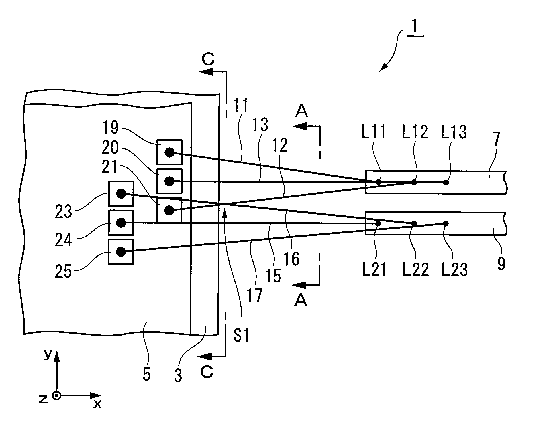
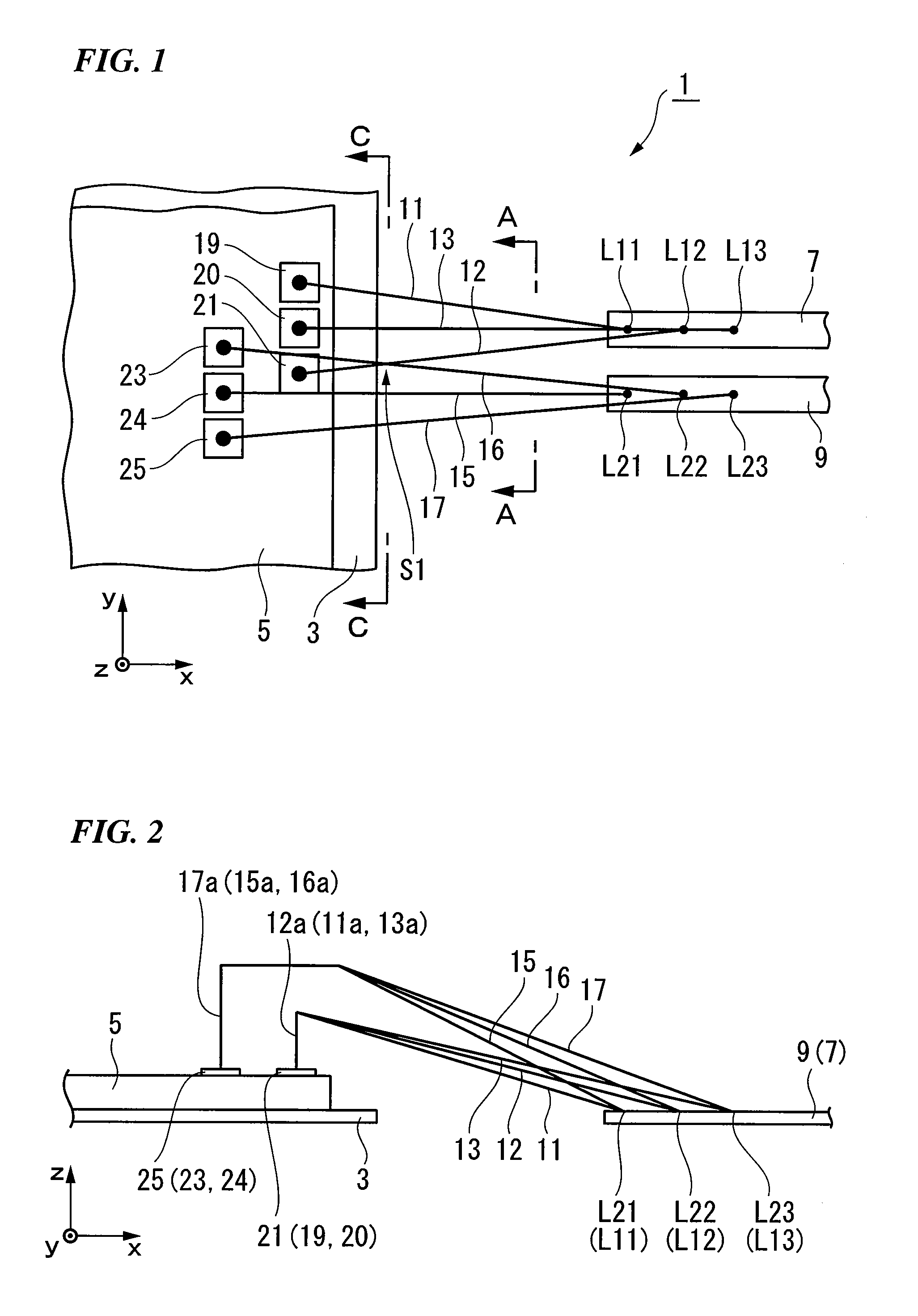
01 Bonding pad metallization structures
Various metallization structures are used for wire bonding pads to improve adhesion, reliability, and electrical performance. These structures typically include multiple layers such as aluminum, copper, titanium, or gold. The metallization stack may include barrier layers to prevent diffusion between metals and adhesion layers to improve bonding strength. The selection of materials and layer thicknesses affects the bonding process and long-term reliability of the interconnection.- Bonding pad metallization structures: The metallization structure of wire bonding pads is critical for ensuring reliable electrical connections in semiconductor devices. Various metal layers and compositions are used to create bonding pads with optimal adhesion, conductivity, and resistance to corrosion. Common metallization structures include aluminum-based pads, copper-based pads with barrier layers, and gold-capped pads. The selection of appropriate metallization depends on the wire material, bonding process parameters, and reliability requirements of the device.
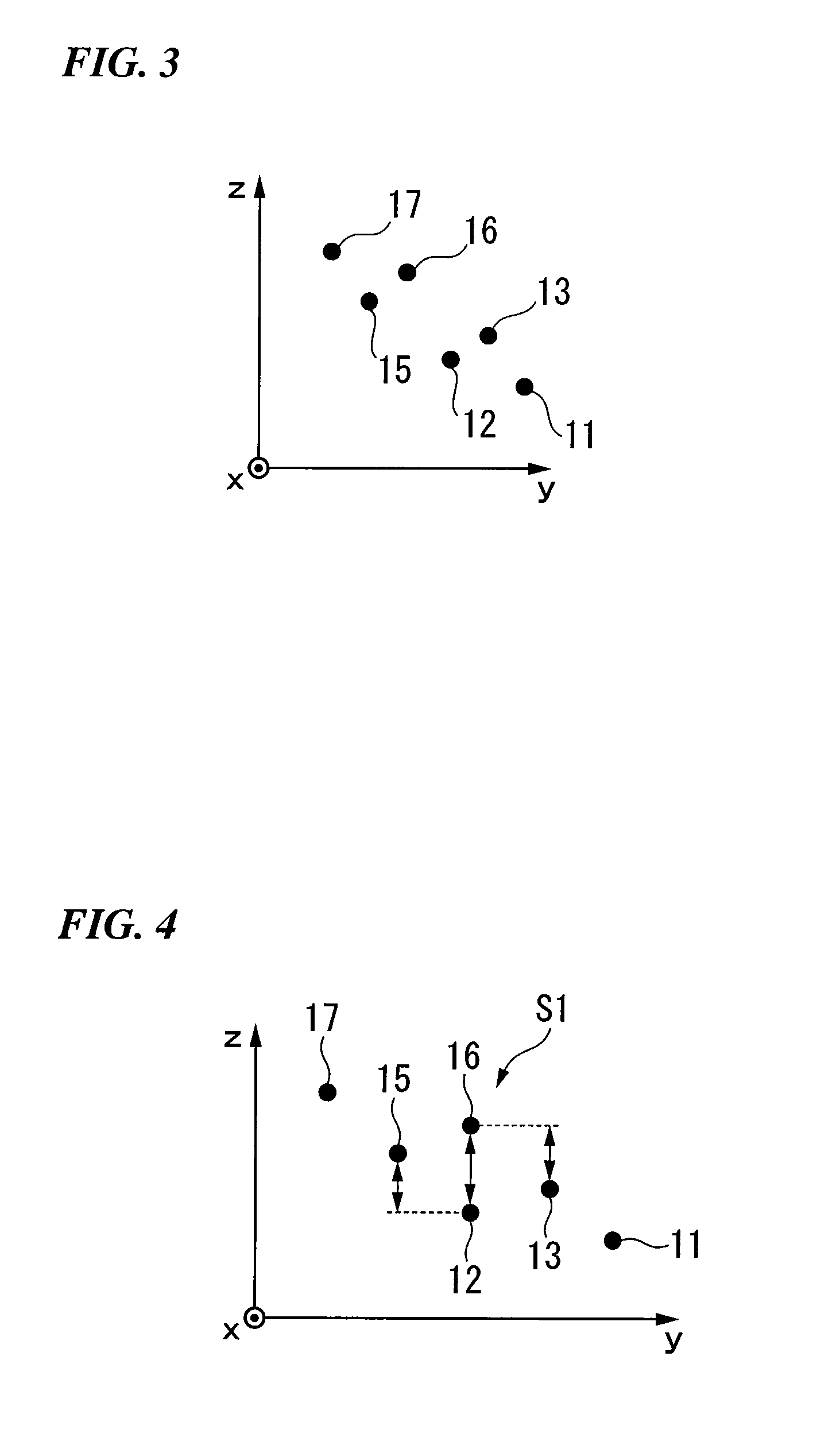
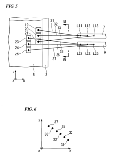
- Wire loop geometry optimization: The geometry of wire bonds significantly impacts the electrical performance and reliability of semiconductor packages. Optimized loop profiles can reduce wire sweep during molding, minimize electrical parasitics, and improve mechanical stability. Various loop shapes such as standard arch, low loop, and reverse bonding are employed depending on the application requirements. Advanced wire bonding equipment allows for precise control of loop height, span, and curvature to accommodate different package designs and performance specifications.
- Pitch limitations and fine pitch bonding: As semiconductor devices continue to shrink, the pitch between adjacent bonding pads becomes increasingly smaller, presenting challenges for wire bonding processes. Fine pitch bonding requires specialized equipment, materials, and techniques to prevent wire sweep and short circuits. The minimum achievable pitch is limited by factors such as wire diameter, bonding tool dimensions, and process capabilities. Advanced techniques like staggered pad arrangements and optimized bonding parameters help overcome these limitations and enable reliable connections at reduced pitches.
- Multi-tier and stacked wire bonding configurations: To accommodate high-density interconnections in advanced semiconductor packages, multi-tier and stacked wire bonding configurations have been developed. These approaches involve bonding wires at different heights or in multiple layers to increase the number of connections without expanding the package footprint. Specialized loop profiles and bonding sequences are employed to prevent wire crossing and short circuits. These techniques are particularly valuable in memory devices, multi-chip modules, and system-in-package applications where high interconnect density is required.
- Advanced materials and processes for wire bonding: Innovations in wire bonding materials and processes continue to enhance the reliability and performance of semiconductor interconnections. These include the development of copper wire as a cost-effective alternative to gold, specialized coatings to improve bondability and reliability, and advanced bonding techniques such as wedge bonding and ribbon bonding. Process monitoring and control systems help maintain consistent bond quality across high-volume production. These advancements enable wire bonding to remain competitive with alternative interconnection technologies while meeting the demands of next-generation semiconductor devices.
02 Wire loop geometry optimization
The geometry of wire bonds significantly impacts package reliability and electrical performance. Loop height, span, and shape are carefully controlled to prevent wire sweep during molding, reduce signal delay, and minimize inductive coupling between adjacent wires. Advanced looping techniques include low-loop profiles for thin packages, reverse bonding for improved reliability, and specialized loop shapes for specific applications. Optimized loop geometry helps maintain wire integrity while meeting package height requirements.Expand Specific Solutions03 Pitch limitation solutions
As semiconductor devices continue to shrink, wire bonding pitch limitations become increasingly challenging. Various approaches address these limitations, including fine-pitch bonding technologies, staggered pad arrangements, and specialized capillary designs. Advanced techniques enable pitches below 40 microns while maintaining reliability. Innovations in wire materials, diameters, and bonding parameters help overcome traditional pitch constraints while ensuring sufficient isolation between adjacent wires to prevent shorts.Expand Specific Solutions04 Pad design for improved bondability
Specific pad designs enhance wire bondability and reliability. Features such as optimized pad size, shape, and surface roughness improve bond strength and consistency. Pad structures may include special openings in passivation layers, reinforcement structures to prevent pad peeling, and controlled oxide thickness for consistent bonding. Some designs incorporate stress-relief features to accommodate thermal expansion differences between the wire and substrate materials, reducing the risk of bond failure during thermal cycling.Expand Specific Solutions05 Advanced materials for high-performance bonding
Novel materials are being developed to enhance wire bonding performance and reliability. These include copper wire as a cost-effective alternative to gold, silver alloys for improved electrical conductivity, and specialized coatings to prevent oxidation and corrosion. Composite wire materials combine the benefits of different metals to achieve optimal electrical, thermal, and mechanical properties. Advanced pad metallization materials are also being developed to improve compatibility with these wire materials and enhance bond strength under various environmental conditions.Expand Specific Solutions
Leading Semiconductor Packaging Companies
Wire bonding technology is currently in a mature phase of industry development, with the global market valued at approximately $4.5 billion and growing steadily at 5-7% annually. The competitive landscape is characterized by established players with specialized expertise in different bonding methodologies. Leading semiconductor manufacturers like Texas Instruments, Samsung Electronics, and NXP Semiconductors have developed proprietary pad metallization techniques optimized for their specific applications. Equipment providers such as Kulicke & Soffa Industries and ASM Technology Singapore dominate the wire bonding machinery segment, continuously pushing pitch limits below 40μm. Advanced Semiconductor Engineering and SMIC lead in implementation services, while materials specialists Tanaka Denshi Kogyo and Heraeus Precious Metals focus on developing specialized wire compositions that enhance both ball and wedge bonding performance across increasingly demanding geometries.
Advanced Semiconductor Engineering, Inc.
Technical Solution: ASE has developed comprehensive wire bonding solutions addressing the technical challenges of both ball and wedge bonding across various semiconductor packaging applications. Their ball bonding technology utilizes a proprietary capillary design that enables fine-pitch applications down to 30μm through precise ball formation control and placement accuracy. ASE has extensively researched pad metallization compatibility, developing specialized surface preparation techniques for copper pad metallization that significantly improve bond strength and reliability. Their CuPlus™ technology incorporates palladium-coated copper wire with optimized bonding parameters that reduce pad cratering issues common in fine-pitch applications. For wedge bonding, ASE employs high-frequency ultrasonic systems (138-148 kHz) that enable aluminum wire bonding at pitches down to 50μm with enhanced process windows. Their loop geometry control system utilizes real-time optical feedback to maintain consistent loop heights as low as 60μm while ensuring sufficient clearance from adjacent wires and components. ASE has also pioneered hybrid bonding approaches that combine the advantages of both ball and wedge techniques for specialized applications.
Strengths: Comprehensive in-house capabilities spanning materials, equipment, and process development; extensive experience with diverse pad metallization schemes including emerging copper-based systems; advanced statistical process control systems that ensure high yields even at pitch limits. Weaknesses: Some proprietary technologies require specialized equipment that limits manufacturing flexibility; certain fine-pitch applications show increased sensitivity to environmental factors during manufacturing; optimization for specific metallization schemes may require significant process development time.
ASM Technology Singapore Pte Ltd.
Technical Solution: ASM Technology has developed the Eagle series wire bonders specifically addressing the challenges of ultra-fine pitch applications for both ball and wedge bonding. Their ball bonding technology incorporates advanced motion control systems with positioning accuracy of ±1.0μm, enabling reliable bonding at pitches down to 35μm. ASM's proprietary Active Bond Force Control™ technology dynamically adjusts bonding parameters based on real-time feedback, compensating for variations in pad metallization and surface conditions. For copper wire ball bonding, they've engineered specialized forming gas delivery systems that prevent oxidation during the ball formation process, critical for consistent intermetallic formation on various pad metallizations including Al, Cu, and Ag-Pd compositions. Their wedge bonding technology utilizes precision-machined wedge tools with optimized geometry that enables aluminum wire bonding at pitches as fine as 45μm. ASM has also developed advanced loop control algorithms that maintain consistent loop profiles across varying bond distances, with capabilities for specialized loop geometries including reverse loops and low-loop profiles as shallow as 50μm for stacked-die applications.
Strengths: Exceptional equipment precision and repeatability enabling consistent performance at pitch limits; advanced software algorithms for loop formation that accommodate complex package geometries; comprehensive process monitoring capabilities that detect and compensate for variations in materials and conditions. Weaknesses: Higher capital equipment costs compared to standard wire bonders; some advanced features require specialized operator training; certain fine-pitch applications may have reduced throughput rates affecting overall productivity.
Critical Patents in Wire Bonding Metallization
Semiconductor device and wire bonding method therefor
PatentInactiveUS20080088012A1
Innovation
- The semiconductor device employs a wire bonding method where wires with varying loop heights are used to connect electrode pads and leads, with one set of wires having a low loop height and the other set having a high loop height, and the use of a small-diameter capillary to form metal bumps and balls, allowing for reduced sizes of bonding pads and contacts while maintaining strong connections.
Wire bonding wedge
PatentInactiveUS7451905B2
Innovation
- The wedge design features sidewalls that constrain the wire's sideways movement while ensuring the foot extends below the sidewalls' level to prevent contact with the overcoat or passivation layer, maintaining wire centrality and avoiding damage, with a curved foot surface and adjustable radius for precise bonding.
Materials Science Advancements for Bond Interfaces
The evolution of wire bonding technology has been significantly influenced by advancements in materials science, particularly at the bond interfaces. Recent developments in pad metallization have revolutionized both ball and wedge bonding processes. Traditional aluminum metallization is increasingly being replaced by copper and gold-based systems that offer superior electrical conductivity and thermal stability. These newer metallization schemes incorporate specialized barrier layers and cap materials that prevent intermetallic compound formation while enhancing bond reliability.
Surface treatments have emerged as critical factors in optimizing bond interfaces. Plasma cleaning techniques now effectively remove organic contaminants and native oxides from pad surfaces, creating more favorable conditions for atomic interdiffusion during the bonding process. Additionally, nano-roughening treatments have been developed to increase the effective surface area of bond pads, enhancing mechanical interlocking between the wire and pad materials.
Composite metallization systems represent another frontier in bond interface technology. These multi-layered structures typically consist of adhesion layers, diffusion barriers, and noble metal caps designed to address specific challenges in high-temperature or corrosive environments. For ball bonding applications, nickel-palladium-gold (Ni/Pd/Au) systems have demonstrated exceptional performance by combining the corrosion resistance of gold with the mechanical strength of the underlying nickel layer.
The microstructural evolution at bond interfaces has been extensively studied using advanced characterization techniques. Transmission electron microscopy and atom probe tomography have revealed that controlled formation of specific intermetallic compounds can actually strengthen bonds rather than degrade them. This understanding has led to the development of thermally optimized bonding processes that promote beneficial microstructural transformations while suppressing detrimental ones.
For fine-pitch applications, novel nanostructured pad materials have been engineered with precisely controlled grain sizes and orientations. These materials exhibit enhanced resistance to electromigration and stress-induced deformation, critical factors in maintaining bond integrity in densely packed semiconductor devices. Complementary advances in wire materials, including doped copper variants and palladium-coated copper, have been specifically designed to interact favorably with these specialized pad metallizations.
The integration of computational materials science has accelerated innovation in this field. Molecular dynamics simulations now accurately predict interfacial reactions between specific wire and pad material combinations, enabling rapid screening of potential metallization systems without extensive experimental testing. This approach has identified promising new alloy compositions that optimize the balance between bondability, reliability, and cost-effectiveness.
Reliability Testing Standards for Wire Bonds
Reliability testing standards for wire bonds are critical frameworks that ensure the long-term performance and durability of interconnections in semiconductor packaging. These standards have evolved significantly over decades, with organizations like JEDEC, MIL-STD, and IPC establishing comprehensive protocols that address various failure mechanisms specific to both ball and wedge bonding technologies.
The primary reliability tests for wire bonds include temperature cycling, high-temperature storage, thermal shock, and humidity testing. Temperature cycling (typically -65°C to +150°C) evaluates bond integrity under thermal expansion coefficient mismatches between different materials. This test is particularly crucial for ball bonds on aluminum pads due to potential intermetallic compound formation that can lead to Kirkendall voiding and eventual failure.
Pull and shear testing represent the cornerstone mechanical evaluations for wire bond reliability. For ball bonds, shear testing (per JEDEC JESD22-B116) measures the force required to shear the ball from the pad surface, while pull testing (JEDEC JESD22-B115) evaluates the overall loop strength. Wedge bonds typically undergo 45° pull tests that assess both the bond interface and wire strength simultaneously.
Electromigration testing has gained prominence particularly for fine-pitch applications, where current densities can reach critical levels. The JEDEC standard JEP154 provides guidelines for electromigration assessment in wire bonds, with ball bonds generally demonstrating superior performance due to their larger contact area compared to wedge bonds.
Accelerated life testing methodologies employ statistical models like Weibull distribution analysis to predict long-term reliability. The Highly Accelerated Stress Test (HAST) combines elevated temperature (130°C) and humidity (85% RH) under bias conditions to accelerate potential electrochemical failures, particularly relevant for aluminum pad metallization with both bonding types.
Recent standards developments have focused on adapting reliability requirements for advanced packaging configurations with finer pitches. The IPC-9701 standard now includes specific provisions for wire bonds below 50μm pitch, addressing unique challenges in loop geometry stability and pad metallization interactions. These updated standards recognize that ball bonding generally permits tighter pitches than wedge bonding, but requires more stringent reliability verification protocols due to the more complex metallurgical interactions at the bond interface.
Unlock deeper insights with Patsnap Eureka Quick Research — get a full tech report to explore trends and direct your research. Try now!
Generate Your Research Report Instantly with AI Agent
Supercharge your innovation with Patsnap Eureka AI Agent Platform!