Wire Bonding On Aluminum Pads: Pad Damage, Cratering And Passivation Integrity
SEP 16, 20259 MIN READ
Generate Your Research Report Instantly with AI Agent
Patsnap Eureka helps you evaluate technical feasibility & market potential.
Wire Bonding Technology Evolution and Objectives
Wire bonding technology has evolved significantly since its inception in the 1950s, becoming the most widely used interconnection method in semiconductor packaging. Initially, the process involved simple thermocompression bonding, which required high temperatures and pressures to form reliable connections. The 1970s witnessed a pivotal advancement with the introduction of ultrasonic and thermosonic bonding techniques, which substantially reduced the required bonding temperatures and improved reliability.
The evolution of wire bonding on aluminum pads has been particularly noteworthy. Aluminum became the preferred pad material due to its excellent electrical conductivity, cost-effectiveness, and compatibility with silicon processing. However, challenges such as pad damage, cratering, and passivation integrity issues emerged as device dimensions decreased and integration densities increased.
Throughout the 1980s and 1990s, significant improvements in wire bonding equipment enabled more precise control over bonding parameters. The introduction of automated vision systems and closed-loop feedback mechanisms allowed for real-time adjustments during the bonding process, reducing the occurrence of pad damage and cratering. Concurrently, advances in metallurgy led to the development of specialized wire alloys that formed stronger bonds while exerting less stress on the underlying pad structures.
The early 2000s marked a transition toward finer pitch capabilities, with bond pad pitches decreasing from over 100μm to below 50μm. This miniaturization trend necessitated innovations in both equipment precision and pad metallization techniques to maintain bond integrity while preventing damage to increasingly delicate pad structures and underlying circuitry.
Recent technological developments have focused on addressing the fundamental mechanisms of pad damage and cratering. Research has revealed that these failures often result from complex interactions between bonding parameters, pad metallization characteristics, and the properties of underlying dielectric layers. Advanced pad designs incorporating stress-absorbing layers and optimized metallization stacks have emerged as effective solutions for enhancing pad robustness.
The primary objectives of current wire bonding technology research include: developing non-destructive testing methods for early detection of potential bond failures; creating predictive models for optimizing bonding parameters based on specific pad designs; improving passivation materials and deposition techniques to enhance interface integrity; and establishing standardized reliability assessment protocols specifically addressing pad damage and cratering phenomena.
Looking forward, the industry aims to achieve zero-defect wire bonding on aluminum pads while simultaneously supporting continued miniaturization and increased functionality in semiconductor devices. This requires a holistic approach that integrates advances in materials science, process control, and equipment design to overcome the persistent challenges of pad damage, cratering, and passivation integrity.
Market Demand for Advanced Wire Bonding Solutions
The global semiconductor packaging market continues to witness substantial growth, with wire bonding remaining a critical interconnection technology despite advancements in flip-chip and other packaging methods. The market demand for advanced wire bonding solutions specifically addressing aluminum pad integrity issues has seen significant expansion, driven by the increasing complexity of semiconductor devices and the push for higher reliability in mission-critical applications.
Semiconductor manufacturers across automotive, aerospace, medical, and consumer electronics sectors are actively seeking solutions that minimize pad damage and cratering while maintaining passivation integrity. This demand is particularly pronounced in the automotive sector, where the average semiconductor content per vehicle has increased dramatically with the rise of electric vehicles and advanced driver assistance systems, requiring higher reliability standards for wire bonding processes.
Market research indicates that approximately one-third of semiconductor packaging failures in high-reliability applications can be attributed to wire bonding issues, with pad damage and cratering representing significant failure modes. This has created a specialized market segment focused on advanced wire bonding technologies that can address these specific challenges while maintaining high throughput and yield rates.
The medical device industry represents another significant growth area for advanced wire bonding solutions, as implantable devices and diagnostic equipment require exceptional reliability and longevity. Manufacturers in this sector are willing to invest in premium wire bonding technologies that can demonstrate superior pad integrity and reduced cratering risk, even at higher initial implementation costs.
Consumer electronics manufacturers, while traditionally more cost-sensitive, are increasingly recognizing the value proposition of advanced wire bonding solutions as device miniaturization continues to push the limits of traditional bonding approaches. The reduction in pad sizes and pitches has exacerbated the challenges of maintaining pad integrity, creating market pull for innovative bonding technologies.
Regional analysis shows particularly strong demand growth in East Asia, where the concentration of semiconductor packaging facilities continues to expand. North American and European markets show more specialized demand patterns focused on high-reliability applications in aerospace, defense, and medical sectors.
The market for specialized equipment, materials, and process control systems addressing aluminum pad integrity has developed into a distinct segment within the broader semiconductor packaging equipment market. Vendors offering comprehensive solutions that combine optimized bonding parameters, advanced monitoring capabilities, and specialized wire materials are gaining market share against traditional equipment providers offering more generalized solutions.
Industry forecasts suggest continued growth in this specialized market segment, with increasing emphasis on solutions that can address the challenges of bonding to ever-thinner aluminum pads while maintaining structural integrity and electrical performance across a wider range of operating conditions.
Aluminum Pad Damage Challenges and Limitations
Aluminum pad damage during wire bonding represents a significant challenge in semiconductor packaging, with implications for device reliability and manufacturing yield. The primary damage mechanisms include cratering, where the pad material fractures beneath the bond, and peeling, where the pad delaminates from the underlying substrate. These failure modes are exacerbated by the increasing miniaturization of semiconductor devices, which necessitates smaller pad sizes while maintaining electrical and mechanical integrity.
The limitations of current aluminum pad technologies become particularly evident when bonding parameters exceed critical thresholds. Ultrasonic energy, bonding force, and temperature—collectively known as the bonding triangle—must be precisely controlled to prevent damage. Excessive ultrasonic energy can cause aluminum grain boundary fracture, while excessive force may transmit stress to underlying structures, potentially damaging active device regions beneath the pad.
Material composition presents another significant limitation. Standard aluminum pads typically contain 1% silicon and 0.5% copper (Al-Si-Cu), offering a balance between electrical conductivity and mechanical strength. However, this composition becomes increasingly inadequate for advanced applications requiring higher current densities or improved electromigration resistance. Alternative metallization schemes such as copper-doped aluminum or aluminum-copper alloys with higher copper content show promise but introduce new integration challenges.
Pad thickness constraints further complicate the bonding process. Industry trends toward thinner metallization layers to reduce parasitic capacitance directly conflict with the mechanical requirements for robust wire bonding. Pads thinner than 0.8μm demonstrate significantly higher susceptibility to cratering and peeling failures, particularly when subjected to gold wire bonding processes that form brittle intermetallic compounds.
Passivation integrity represents another critical limitation. Modern devices utilize complex passivation stacks including materials like silicon nitride, silicon oxynitride, and polyimide. These materials must withstand the mechanical and thermal stresses of the bonding process while maintaining hermeticity. Cracks in passivation layers can propagate during thermal cycling, creating pathways for moisture ingress and subsequent corrosion of the aluminum pad and interconnect structures.
The industry faces additional challenges with pad design rules that must balance electrical performance with mechanical robustness. Pad-to-pad spacing, pad geometry, and underlying metal routing all influence bonding reliability. Particularly problematic are designs where metal traces run beneath bond pads, creating stress concentration points that can initiate cratering failures during the bonding process or subsequent reliability testing.
Current Methodologies for Preventing Pad Cratering
01 Pad structure modifications to prevent cratering
Modifying the structure of aluminum bond pads can significantly reduce the risk of cratering during wire bonding. These modifications include using multi-layered pad structures, incorporating barrier layers, and optimizing pad thickness. Specialized pad designs with reinforced structures can distribute bonding forces more evenly, preventing damage to underlying layers. These structural improvements help maintain the integrity of the pad while ensuring good electrical connectivity.- Pad structure modifications to prevent cratering: Modifications to the aluminum pad structure can prevent cratering during wire bonding. These include using multi-layered pad structures with barrier metals, optimizing pad thickness, and incorporating reinforcement layers beneath the aluminum. These structural enhancements distribute bonding forces more evenly, reducing stress concentration that leads to cratering and maintaining passivation integrity around the bond area.
- Wire bonding process optimization: Optimizing the wire bonding process parameters is crucial for preventing pad damage. This includes controlling bonding force, ultrasonic power, bonding time, and temperature. Proper calibration of these parameters ensures sufficient bond strength while minimizing mechanical stress on the aluminum pad. Advanced techniques such as stepped force profiles and optimized ultrasonic energy delivery can significantly reduce cratering and maintain passivation integrity.
- Passivation design and integrity preservation: Proper passivation design around bond pads is essential for maintaining integrity during wire bonding. This includes optimizing passivation thickness, using materials with appropriate mechanical properties, and implementing specific edge designs around the pad opening. Advanced passivation structures with stress-relief features can prevent cracks and delamination during the bonding process, ensuring long-term reliability of the interconnection.
- Surface treatment of aluminum pads: Surface treatments of aluminum pads can significantly improve wire bonding reliability. These include plasma cleaning, chemical etching, and thermal treatments to remove oxides and contaminants. Some approaches involve creating controlled surface textures or applying thin metal finishes to enhance bond adhesion. These treatments optimize the interface between the bond wire and pad surface, reducing the force needed for successful bonding and minimizing pad damage.
- Advanced pad metallization schemes: Advanced metallization schemes for bond pads can prevent damage during wire bonding. These include using composite structures with cap layers, alloying aluminum with copper or silicon, and implementing diffusion barriers. Some approaches utilize specialized under-bump metallization or redistribution layers. These metallization strategies enhance pad hardness and durability while maintaining excellent electrical conductivity and bondability.
02 Passivation layer design for improved integrity
Proper design of passivation layers around aluminum bond pads is crucial for maintaining integrity during wire bonding. Techniques include optimizing passivation openings, using specialized materials with better adhesion properties, and implementing multi-layer passivation schemes. The passivation edge design significantly impacts stress distribution during bonding, with tapered or stepped profiles reducing the risk of cracking and delamination. These approaches ensure that the passivation remains intact during the thermal and mechanical stresses of the bonding process.Expand Specific Solutions03 Wire bonding process optimization
Optimizing the wire bonding process parameters can significantly reduce pad damage and cratering. This includes controlling bonding force, ultrasonic power, bonding time, and temperature. Advanced bonding techniques such as pulsed thermosonic bonding and variable force profiles can minimize stress on aluminum pads. Proper calibration of bonding equipment and selection of appropriate bonding tools based on pad size and material are also essential for preventing damage while ensuring reliable connections.Expand Specific Solutions04 Metallization techniques for enhanced pad strength
Advanced metallization techniques can enhance the strength and reliability of aluminum bond pads. These include alloying aluminum with copper or silicon, implementing specialized deposition methods, and post-deposition treatments. Surface treatments such as plasma cleaning and annealing can improve the bonding interface quality. Multi-metal systems with barrier layers prevent intermetallic formation and enhance adhesion between the pad and wire, reducing the likelihood of cratering and ensuring long-term reliability.Expand Specific Solutions05 Inspection and testing methods for pad damage prevention
Implementing effective inspection and testing methods is crucial for preventing and detecting pad damage. Non-destructive testing techniques such as acoustic microscopy and X-ray inspection can identify potential issues before they cause failures. In-process monitoring systems that analyze bonding parameters in real-time allow for immediate adjustments to prevent damage. Statistical process control and failure analysis methodologies help identify root causes of pad damage, enabling continuous improvement of bonding processes and pad designs to enhance overall reliability.Expand Specific Solutions
Key Manufacturers and Suppliers in Wire Bonding Industry
Wire bonding on aluminum pads presents a competitive landscape in the mature semiconductor packaging industry, currently valued at approximately $25 billion globally. The market is in a consolidation phase, with established players like Taiwan Semiconductor Manufacturing Co., Infineon Technologies, and Texas Instruments leading technological advancements in addressing pad damage and cratering issues. Companies such as Kulicke & Soffa Industries and Tanaka Denshi Kogyo have developed specialized solutions for passivation integrity challenges. The technology has reached high maturity levels, with recent innovations focusing on ultra-fine pitch applications and improved reliability for automotive and high-performance computing applications. NXP, Samsung Electronics, and GlobalFoundries are investing in advanced materials and process optimizations to minimize aluminum pad damage during high-volume manufacturing.
Taiwan Semiconductor Manufacturing Co., Ltd.
Technical Solution: TSMC has developed a comprehensive approach to aluminum pad integrity during wire bonding processes. Their technology focuses on a multi-layered pad structure design that incorporates specialized barrier metals and optimized aluminum composition to enhance pad durability. TSMC's proprietary pad structure includes carefully engineered thickness ratios between aluminum and underlying metals, creating a stress-absorption mechanism that prevents cratering. Their research has demonstrated that controlling aluminum grain size and orientation significantly impacts bonding reliability. TSMC implements advanced passivation techniques using specialized silicon nitride and polyimide materials that maintain integrity even under high bonding stresses. The company has also developed proprietary pre-bond surface treatments that remove native oxides while preserving pad structure. Their integrated approach includes customized bonding parameter optimization based on specific pad designs, with real-time monitoring systems that can detect potential cratering issues before they become critical failures. TSMC's research indicates their enhanced pad structures can withstand up to 30% higher bonding forces without compromising reliability.
Strengths: Comprehensive integration of pad design, materials science, and process optimization; extensive manufacturing experience across diverse semiconductor applications; advanced quality control systems. Weaknesses: Solutions often tailored to high-volume manufacturing environments; implementation may require significant process modifications for existing production lines.
Infineon Technologies AG
Technical Solution: Infineon has pioneered advanced aluminum pad structures specifically engineered to withstand wire bonding stresses. Their technology incorporates a gradient-based metallization approach where the aluminum pad composition gradually changes with depth, creating a more resilient structure against mechanical stress. Infineon's research has focused on optimizing pad thickness and underlying metal stack configurations to distribute bonding forces more effectively. Their proprietary "FlexBond" technology implements adaptive bonding parameters that adjust in real-time based on feedback from the bonding process, significantly reducing cratering incidents. Infineon has developed specialized passivation materials with enhanced adhesion properties that maintain integrity even under extreme bonding conditions. Their approach includes comprehensive pad design rules that account for both electrical performance and mechanical reliability. The company's research has demonstrated that their optimized pad structures can reduce cratering failures by up to 35% compared to conventional designs. Infineon also employs advanced simulation techniques to predict stress distribution during bonding, allowing for pre-emptive design modifications before manufacturing.
Strengths: Strong integration between device design and manufacturing processes; extensive experience in automotive and industrial applications requiring high reliability; comprehensive failure analysis capabilities. Weaknesses: Some solutions may require specialized equipment configurations; implementation complexity can increase for very fine-pitch applications.
Critical Patents in Aluminum Pad Integrity Preservation
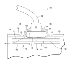
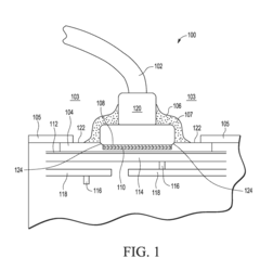
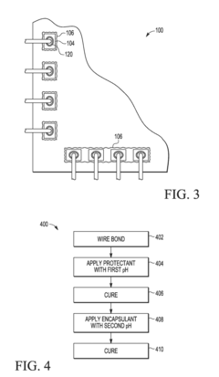
Semiconductor device with protective material and method for encapsulating
PatentActiveUS20170040282A1
Innovation
- A protective material with a neutral to mildly alkaline pH is applied over copper wire bonds on aluminum pads to neutralize corrosive contaminants in the encapsulating material, preventing corrosion of intermetallic layers and enhancing the reliability of copper wire bonds.
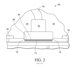
An integrated circuit device
PatentInactiveEP1051750B1
Innovation
- The bond pads' circuit-connecting region is situated outside the wire-bonding region, with a continuous inorganic passivating material layer beneath, eliminating the need for organic materials by optimizing the thicknesses of the passivating material and bond pads to withstand bonding forces.
Reliability Testing Standards for Wire Bond Connections
Reliability testing standards for wire bond connections have evolved significantly over the past decades to address the critical challenges in microelectronic packaging. These standards primarily focus on ensuring the mechanical integrity, electrical performance, and long-term reliability of wire bonds under various environmental and operational conditions.
The Joint Electron Device Engineering Council (JEDEC) has established comprehensive standards such as JESD22-B116 for wire bond shear testing and JESD22-B107 for wire bond pull testing. These standards define precise methodologies for evaluating bond strength and detecting potential failures in aluminum pad connections.
Military standards like MIL-STD-883 Method 2011 provide rigorous testing protocols specifically designed for high-reliability applications in aerospace and defense sectors. These standards incorporate detailed procedures for bond pull testing with specific force requirements based on wire diameter and material composition.
The Automotive Electronics Council (AEC) has developed AEC-Q100 qualification requirements that include specialized reliability testing for wire bonds in automotive applications. These standards address the unique challenges of temperature cycling, vibration, and humidity that automotive electronics encounter.
Temperature cycling tests (JESD22-A104) are particularly critical for evaluating aluminum pad integrity, as they reveal potential cratering and passivation failures that might occur due to coefficient of thermal expansion mismatches between the wire and pad materials. These tests typically involve cycling between extreme temperatures (-65°C to +150°C) for hundreds or thousands of cycles.
High-temperature operating life (HTOL) testing standards (JESD22-A108) evaluate long-term reliability by subjecting wire bonds to elevated temperatures while under electrical bias. This accelerated aging test helps identify potential intermetallic compound formation issues at the aluminum pad interface.
Humidity testing standards (JESD22-A101) assess the susceptibility of wire bonds to moisture-induced corrosion and degradation, which can significantly impact aluminum pad integrity and bond reliability over time.
The International Electrotechnical Commission (IEC) has established IEC 60749 standards that provide globally recognized test methods for semiconductor devices, including specific procedures for evaluating wire bond reliability on various pad materials including aluminum.
These standardized testing methodologies incorporate statistical analysis requirements to ensure meaningful data interpretation, typically requiring minimum sample sizes and defining acceptable failure rates based on application criticality.
Environmental Impact of Wire Bonding Materials
The environmental impact of wire bonding materials has become increasingly significant as semiconductor manufacturing volumes continue to grow globally. Traditional wire bonding processes primarily utilize gold, aluminum, and copper wires, each carrying distinct environmental footprints throughout their lifecycle. Gold wire bonding, while offering excellent reliability and performance, presents substantial environmental concerns due to resource-intensive mining operations that contribute to habitat destruction, water pollution, and high energy consumption. The extraction of one ounce of gold can generate up to 20 tons of waste material, making it one of the most environmentally costly materials in semiconductor packaging.
Aluminum wire bonding offers a more environmentally favorable alternative, requiring approximately 85% less energy to produce compared to gold. The aluminum extraction process, while still impactful, generates significantly fewer greenhouse gas emissions and toxic byproducts. However, the pad damage and cratering issues associated with aluminum bonding often necessitate rework and scrapping of components, indirectly increasing the environmental burden through manufacturing waste.
Copper wire has emerged as an eco-friendlier option with a 30% lower carbon footprint than gold while maintaining comparable electrical performance. The transition toward copper bonding represents a positive environmental trend, though challenges remain regarding oxidation resistance and the need for specialized pad metallization to prevent cratering and ensure passivation integrity.
The chemical compounds used in pad preparation and passivation layers also contribute to environmental concerns. Many traditional passivation materials contain perfluorinated compounds (PFCs) and other persistent chemicals that resist environmental degradation. When improperly disposed of, these substances can contaminate water systems and accumulate in living organisms, presenting long-term ecological risks.
End-of-life considerations reveal additional environmental challenges. The complex integration of bonding materials with aluminum pads and passivation layers makes recycling difficult, with less than 15% of precious metals from electronic components being successfully recovered. The remainder typically ends up in landfills where metal leaching can occur, potentially contaminating soil and groundwater.
Recent industry initiatives have focused on developing more sustainable wire bonding approaches, including lead-free alternatives and biodegradable passivation materials. Several manufacturers have implemented closed-loop water systems for wire bonding processes, reducing water consumption by up to 60%. Additionally, advanced recycling technologies specifically designed for semiconductor packaging materials show promise for improving recovery rates of valuable metals while minimizing environmental impact.
Unlock deeper insights with Patsnap Eureka Quick Research — get a full tech report to explore trends and direct your research. Try now!
Generate Your Research Report Instantly with AI Agent
Supercharge your innovation with Patsnap Eureka AI Agent Platform!