

Wire Bonding Vs Flip-Chip Interconnects: Cost, Reliability And Operating Windows
SEP 16, 20259 MIN READ
Generate Your Research Report Instantly with AI Agent
PatSnap Eureka helps you evaluate technical feasibility & market potential.
Interconnect Technologies Background and Objectives
Interconnect technology has evolved significantly over the past several decades, transitioning from simple wire connections to sophisticated integration methods that enable today's advanced electronic devices. Wire bonding, developed in the 1950s, represents the traditional approach for connecting semiconductor dies to package substrates. This technology has matured through various iterations including gold, aluminum, and copper wire implementations, each offering specific advantages in terms of cost, performance, and reliability.
Flip-chip technology emerged in the 1960s as an alternative interconnection method, initially pioneered by IBM under the name Controlled Collapse Chip Connection (C4). Unlike wire bonding which creates connections at the perimeter of the die, flip-chip technology utilizes the entire die surface area for interconnections, enabling higher I/O density and improved electrical performance through shorter connection paths.
The semiconductor industry's relentless pursuit of miniaturization, increased functionality, and enhanced performance has driven continuous innovation in interconnect technologies. Moore's Law has pushed package dimensions smaller while simultaneously demanding more connections, creating significant technical challenges for traditional interconnect methods.
The primary objective of this technical research is to conduct a comprehensive comparative analysis of wire bonding and flip-chip interconnect technologies across three critical dimensions: cost structures, reliability metrics, and operational parameters. This analysis aims to provide actionable insights for technology selection based on specific application requirements and production constraints.
Cost considerations include not only the direct material and equipment expenses but also indirect factors such as throughput capabilities, yield rates, and rework possibilities. The reliability assessment encompasses thermal cycling performance, mechanical stress resistance, and long-term stability under various environmental conditions. Operating windows analysis focuses on the technical limitations and capabilities of each technology, including pitch constraints, I/O count maximums, and thermal management characteristics.
This research will examine how these interconnect technologies perform across different application domains, from consumer electronics to automotive systems and high-reliability aerospace applications. The findings will help inform strategic technology roadmaps and investment decisions for semiconductor packaging operations.
Additionally, this study will explore emerging hybrid approaches that combine elements of both technologies to address specific application challenges, as well as potential future developments in interconnect technology that may eventually supersede both wire bonding and flip-chip methods in certain market segments.
Market Demand Analysis for Advanced Packaging Solutions
The semiconductor packaging market is experiencing a significant shift towards advanced interconnect technologies, driven by the increasing demand for higher performance, smaller form factors, and greater reliability in electronic devices. The global advanced packaging market is projected to reach $42.73 billion by 2027, growing at a CAGR of 10.2% from 2020 to 2027, with interconnect technologies playing a crucial role in this expansion.
Wire bonding has traditionally dominated the semiconductor packaging landscape, accounting for approximately 75-80% of all semiconductor interconnections. This dominance stems from its cost-effectiveness, process maturity, and flexibility. However, market analysis indicates a gradual shift towards flip-chip technology, particularly in high-performance applications where electrical performance and miniaturization are paramount.
The consumer electronics sector represents the largest market segment for advanced interconnect technologies, with smartphones alone requiring billions of interconnects annually. The transition from wire bonding to flip-chip in premium smartphones has been accelerating, with major manufacturers adopting flip-chip technology for their flagship devices to achieve thinner profiles and better performance.
Automotive electronics presents another rapidly growing market segment, expected to grow at a CAGR of 12.5% through 2026. The increasing electronic content in vehicles, particularly in electric and autonomous vehicles, demands more reliable interconnect solutions that can withstand harsh operating environments. Flip-chip interconnects are gaining traction in safety-critical automotive applications due to their superior reliability under thermal cycling and mechanical stress.
Data centers and high-performance computing applications represent a premium market segment where performance considerations often outweigh cost factors. This segment has been an early adopter of flip-chip technology due to its superior electrical performance and heat dissipation capabilities. The exponential growth in cloud computing and AI applications continues to drive demand for advanced interconnect solutions in this sector.
Market research indicates regional variations in adoption patterns. While North America and Europe lead in flip-chip adoption for high-end applications, Asia-Pacific remains the largest market for both technologies, with China, Taiwan, and South Korea serving as manufacturing hubs. The region's diverse electronics manufacturing ecosystem supports both mature wire bonding processes and cutting-edge flip-chip implementations.
Industry surveys reveal that cost remains the primary consideration for manufacturers when selecting interconnect technology, particularly for consumer products with tight margins. However, reliability concerns are increasingly influencing decision-making, especially in automotive, aerospace, and medical device sectors where failure costs extend beyond the component itself.
Current State and Challenges in Chip Interconnection
The semiconductor industry is currently witnessing a significant transition in chip interconnection technologies, with Wire Bonding and Flip-Chip techniques representing the two dominant approaches. Wire bonding, the traditional method dating back to the 1950s, continues to hold approximately 75-80% of the market share due to its cost-effectiveness and process maturity. Meanwhile, flip-chip technology has gained substantial traction in high-performance applications, capturing about 20-25% of the market with continued growth projected.
Globally, the distribution of these technologies shows regional specialization patterns. East Asian countries, particularly Taiwan, South Korea, and Japan, have established dominance in advanced flip-chip manufacturing, while China maintains significant wire bonding capacity. North America and Europe focus primarily on specialized high-performance applications utilizing both technologies, with particular emphasis on flip-chip for cutting-edge devices.
The current technical landscape presents several critical challenges. For wire bonding, the primary limitations include increasing I/O density requirements that exceed physical spacing constraints, signal integrity issues at higher frequencies, and thermal management concerns. The technology struggles to meet the demands of devices operating above 10GHz, where parasitic inductance becomes prohibitive.
Flip-chip technology, while addressing many wire bonding limitations, faces its own set of challenges. Manufacturing complexity and initial capital investment requirements remain significant barriers to wider adoption. The need for precise bump placement and underfill processes increases production complexity, while thermal expansion mismatches between silicon dies and organic substrates create reliability concerns in harsh operating environments.
Cost considerations continue to drive technology selection decisions. Wire bonding maintains a 30-50% cost advantage for low to medium I/O applications, making it the preferred choice for consumer electronics and automotive applications where cost sensitivity is paramount. Conversely, flip-chip technology, despite higher initial costs, offers superior performance that justifies its use in high-end computing, telecommunications, and military applications.
Reliability testing reveals distinct failure modes for each technology. Wire bonds typically fail through wire fatigue, heel cracks, or bond pad cratering under thermal cycling conditions. Flip-chip interconnects more commonly experience solder joint cracking, underfill delamination, or substrate warpage. Recent reliability studies indicate flip-chip assemblies generally demonstrate superior performance under thermal cycling conditions, while wire bonding may offer advantages in drop-test scenarios depending on specific implementation details.
The operating windows for these technologies continue to evolve, with wire bonding facing increasing limitations as frequencies exceed 5GHz and I/O counts surpass 1000 pins. Flip-chip technology extends these boundaries significantly but introduces new manufacturing precision requirements and thermal management considerations that must be addressed through advanced materials and process innovations.
Comparative Analysis of Wire Bonding and Flip-Chip Solutions
01 Cost comparison between wire bonding and flip-chip interconnects
Wire bonding and flip-chip interconnects have different cost structures in semiconductor packaging. Wire bonding typically has lower initial equipment costs and is more flexible for low-volume production, making it cost-effective for certain applications. Flip-chip technology, while having higher upfront costs for equipment and materials, can offer better cost efficiency in high-volume production due to its parallel processing capabilities and reduced package size. The overall cost comparison depends on factors such as production volume, die size, I/O count, and performance requirements.- Cost comparison between wire bonding and flip-chip interconnects: Wire bonding and flip-chip technologies have different cost structures in semiconductor packaging. Wire bonding is generally considered more cost-effective for lower I/O count applications due to its mature process and equipment infrastructure. Flip-chip technology, while initially more expensive due to higher capital equipment costs and more complex processing, can be more economical for high-density interconnects and may offer lower total system costs when considering electrical performance improvements and package size reduction.
- Reliability factors in interconnect technologies: Reliability is a critical consideration when choosing between wire bonding and flip-chip interconnects. Wire bonding reliability can be affected by wire sweep, bond strength, and thermal cycling performance. Flip-chip interconnects generally offer better reliability under thermal cycling conditions due to their shorter electrical paths and more uniform stress distribution. However, they may face challenges related to underfill delamination, solder joint fatigue, and coefficient of thermal expansion (CTE) mismatches between the die and substrate.
- Operating windows and process parameters: The operating windows for wire bonding and flip-chip processes define the range of parameters within which reliable interconnects can be formed. For wire bonding, key parameters include bonding force, ultrasonic power, temperature, and time. The flip-chip process operating window is influenced by factors such as solder composition, reflow profile, underfill properties, and bump geometry. Understanding these operating windows is essential for optimizing process yield and ensuring consistent interconnect performance across various environmental conditions.
- Advanced packaging solutions combining interconnect technologies: Hybrid and advanced packaging solutions often combine wire bonding and flip-chip technologies to leverage the advantages of each. These approaches include package-on-package (PoP), system-in-package (SiP), and 2.5D/3D integration. By strategically applying the appropriate interconnect technology for different components within a system, manufacturers can optimize performance, reliability, and cost. These hybrid solutions are particularly valuable for complex systems requiring high performance in compact form factors.
- Material innovations for improved interconnect performance: Material innovations are driving improvements in both wire bonding and flip-chip interconnect technologies. For wire bonding, developments include copper wire as a cost-effective alternative to gold, and silver alloys for enhanced reliability. In flip-chip technology, lead-free solder compositions, copper pillar bumps, and advanced underfill materials are enhancing performance and reliability. These material innovations help address thermal management challenges, improve electrical performance, and extend the operating life of semiconductor packages.
02 Reliability factors in interconnect technologies
Reliability is a critical consideration when choosing between wire bonding and flip-chip interconnects. Wire bonding reliability can be affected by wire sweep, bond strength, and thermal cycling resistance. Flip-chip interconnects generally offer better mechanical stability and thermal performance due to shorter electrical paths and direct die-to-substrate connections. However, they may face challenges with coefficient of thermal expansion (CTE) mismatch and underfill reliability. Both technologies have evolved to address their respective reliability concerns through improved materials, process controls, and design optimizations.Expand Specific Solutions03 Operating windows and process parameters
The operating windows for wire bonding and flip-chip interconnects are defined by various process parameters that must be controlled to ensure quality connections. For wire bonding, critical parameters include bonding force, ultrasonic power, bonding time, and temperature. The operating window for flip-chip technology is influenced by factors such as bump height uniformity, reflow temperature profile, underfill flow characteristics, and substrate planarity. Advanced process control systems and inspection methods are employed to maintain these parameters within acceptable ranges, ensuring consistent interconnect quality and reliability.Expand Specific Solutions04 Thermal performance and electrical characteristics
Wire bonding and flip-chip interconnects exhibit different thermal and electrical performance characteristics. Flip-chip technology generally provides superior thermal dissipation due to the shorter thermal path between the die and substrate, making it advantageous for high-power applications. Electrically, flip-chip connections offer lower inductance, resistance, and capacitance compared to wire bonds, resulting in better high-frequency performance and signal integrity. These thermal and electrical advantages make flip-chip particularly suitable for high-performance computing, RF applications, and power electronics, while wire bonding remains viable for less demanding applications.Expand Specific Solutions05 Advanced packaging solutions combining interconnect technologies
The semiconductor industry has developed hybrid and advanced packaging solutions that leverage the strengths of both wire bonding and flip-chip interconnects. These include package-on-package (PoP) configurations, system-in-package (SiP) designs, and 2.5D/3D integration approaches. Some solutions use flip-chip for high-density core connections while employing wire bonding for peripheral connections or stacked dies. These hybrid approaches optimize cost, reliability, and performance trade-offs, allowing for customized solutions that meet specific application requirements while addressing the limitations of each individual interconnect technology.Expand Specific Solutions
Key Industry Players in Interconnect Manufacturing
The wire bonding vs flip-chip interconnect market is in a mature growth phase, with the global semiconductor packaging market valued at approximately $30 billion. While wire bonding remains dominant due to cost advantages and established infrastructure, flip-chip technology is gaining momentum for high-performance applications requiring superior electrical characteristics and thermal management. The competitive landscape features established players like TSMC, Intel, and Samsung leading flip-chip adoption, while companies such as Texas Instruments and NXP maintain significant wire bonding operations. Tessera and Qualcomm are advancing packaging innovations, with research institutions like A*STAR and Nanyang Technological University contributing to technological advancements. The market is experiencing a gradual shift toward flip-chip for premium applications, though wire bonding continues to dominate cost-sensitive segments.
Intel Corp.
Technical Solution: Intel employs advanced flip-chip technology called Embedded Multi-die Interconnect Bridge (EMIB) that provides high-density die-to-die connections without the need for silicon interposers. This approach embeds small silicon bridges into the package substrate to connect multiple dies with thousands of fine-pitch micro-bumps. Intel's flip-chip technology utilizes copper pillars with solder caps at pitches below 50μm, enabling high-bandwidth connections between dies. For their lower-cost products, Intel maintains wire bonding capabilities using both gold and copper wires, with proprietary loop profile control algorithms to optimize electrical performance and reliability. Intel has demonstrated reliability improvements in their flip-chip technology through underfill optimization and stress management techniques that reduce thermal cycling failures by up to 65% compared to conventional approaches.
Strengths: EMIB technology offers interposer-like performance at lower cost; excellent electrical and thermal performance in high-performance computing applications. Weaknesses: Higher implementation complexity; requires specialized equipment and processes; less flexible for package modifications after assembly compared to wire bonding.
QUALCOMM, Inc.
Technical Solution: Qualcomm has developed a hybrid approach combining both wire bonding and flip-chip technologies in their RF modules and mobile SoCs. Their RF360 front-end modules utilize flip-chip for the main processor die while employing wire bonding for peripheral components, optimizing both performance and cost. Qualcomm's flip-chip technology features copper pillar bumps with pitches down to 40μm and has implemented wafer-level packaging techniques to reduce form factors. For their mobile processors, Qualcomm employs Package-on-Package (PoP) configurations with flip-chip connections to the substrate and wire bonding for memory integration. Their reliability enhancement techniques include specialized underfill materials that reduce coefficient of thermal expansion (CTE) mismatch stress by approximately 30%, extending thermal cycling lifetime significantly compared to standard materials.
Strengths: Optimized hybrid solutions balancing performance and cost; excellent RF performance in flip-chip implementations; high volume manufacturing expertise. Weaknesses: Complex supply chain management required for hybrid approaches; thermal management challenges in densely packed mobile processors.
Critical Patents and Technical Literature in Interconnect Methods
Integrated circuit system for bonding
PatentInactiveUS20060231948A1
Innovation
- A chemical etchant solution containing a viscosity modifier, such as propylene glycol, and an oxidizer, like hydrogen peroxide, is used to etch the Ti layer, improving selectivity over Al and preventing Ti residue on the passivation layer, thereby preserving the Al pads for wire bonding.
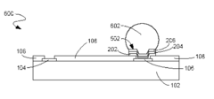
Flip-Chip Interconnect Structure
PatentInactiveUS20090108443A1
Innovation
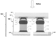
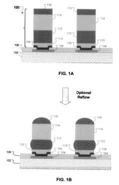
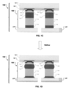
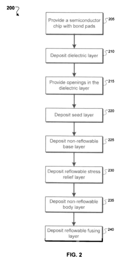
- The implementation of a flip-chip interconnect structure with a stress relief means, comprising a non-reflowable base layer, a reflowable stress relief layer, and a reflowable fusing layer, which acts as a shock absorber to alleviate mechanical stresses, using materials like copper, nickel, and solder alloys, and allowing for controlled collapsible solder bumps without the need for solder dams or pre-reflow processes.
Cost-Performance Trade-offs in Interconnect Selection
The selection between wire bonding and flip-chip interconnect technologies presents significant cost-performance trade-offs that must be carefully evaluated by manufacturers. Wire bonding typically offers lower initial capital investment, with equipment costs ranging from $500,000 to $2 million, compared to flip-chip systems that can exceed $5 million. This substantial difference in upfront investment makes wire bonding particularly attractive for small to medium production volumes and startups with limited capital resources.
Manufacturing throughput considerations further complicate the decision matrix. Wire bonding processes operate at speeds of 5-12 wires per second, while advanced flip-chip systems can place thousands of bumps simultaneously. This throughput advantage for flip-chip becomes increasingly significant as production volumes scale, effectively amortizing the higher initial equipment costs across larger unit volumes.
Material costs present another critical dimension in the trade-off analysis. Wire bonding utilizes gold, copper, or aluminum wires that range from $0.10 to $1.50 per device depending on complexity and wire material. Flip-chip processes require specialized under-bump metallization (UBM), solder materials, and underfill compounds, typically costing $0.30 to $2.00 per device. However, flip-chip's smaller form factor can reduce substrate costs by 15-30%, potentially offsetting some of these additional material expenses.
Performance benefits of flip-chip technology include superior electrical characteristics with 50-70% lower inductance, 20-40% better thermal performance, and significantly reduced signal propagation delays. These advantages become increasingly valuable in high-frequency applications above 2GHz and in power-intensive devices where thermal management is critical.
Reliability metrics reveal that flip-chip interconnects typically demonstrate mean time between failures (MTBF) rates 2-3 times higher than wire bonds under thermal cycling conditions. However, wire bonding maintains advantages in shock resistance and vibration tolerance, making it preferable for automotive and industrial applications experiencing mechanical stress.
The total cost of ownership calculation must incorporate yield considerations, with mature wire bonding processes achieving yields of 99.7-99.9%, while flip-chip processes typically range from 99.0-99.7%. This yield differential can significantly impact effective unit costs, especially for high-value components where each percentage point in yield represents substantial revenue.
For next-generation applications requiring miniaturization, high-frequency operation, or advanced thermal management, the performance premium of flip-chip technology increasingly justifies its higher cost structure, despite the more favorable initial economics of wire bonding solutions.
Thermal Management Considerations for Different Interconnects
Thermal management represents a critical factor in the selection and implementation of interconnect technologies, with significant differences between wire bonding and flip-chip approaches. Wire bonding creates a longer thermal path from the die to the package substrate, resulting in higher thermal resistance. This configuration typically yields junction-to-case thermal resistance values ranging from 10-30°C/W, depending on die size and bond wire configuration. The elevated thermal resistance can lead to localized hotspots at the wire-die interface, potentially accelerating electromigration and reducing overall reliability under high-power operating conditions.
In contrast, flip-chip interconnects offer superior thermal performance due to their direct die-to-substrate connection. The shorter thermal path reduces junction-to-case thermal resistance to approximately 3-8°C/W, representing a 3-4x improvement over wire bonding. This enhanced thermal efficiency enables flip-chip packages to handle significantly higher power densities, making them particularly advantageous for high-performance computing applications where thermal management is paramount.
The thermal dissipation capabilities of each interconnect technology directly impact their respective operating windows. Wire bonded devices typically operate reliably up to 125°C junction temperature, with performance degradation accelerating beyond this threshold. Flip-chip interconnects, with their superior thermal characteristics, can maintain reliable operation at junction temperatures up to 150°C in standard configurations, with specialized high-temperature variants extending this range further.
Environmental considerations also influence thermal management strategies for different interconnects. Wire bonded packages often require additional heat spreaders or specialized thermal interface materials to compensate for their inherent thermal limitations. Flip-chip implementations can leverage more direct cooling solutions, including integrated heat spreaders and direct liquid cooling approaches, further extending their thermal performance advantage.
Recent advancements in thermal management for wire bonding include the development of thermally enhanced molding compounds and the strategic placement of thermal vias beneath bond pads. For flip-chip interconnects, innovations focus on underfill materials with improved thermal conductivity and the integration of microfluidic cooling channels within the substrate. These developments aim to narrow the thermal performance gap between the two technologies while addressing their specific thermal management challenges.
Unlock deeper insights with PatSnap Eureka Quick Research — get a full tech report to explore trends and direct your research. Try now!
Generate Your Research Report Instantly with AI Agent
Supercharge your innovation with PatSnap Eureka AI Agent Platform!