Electrostatic protection structure of image sensor and image sensor

An image sensor, electrostatic protection technology, applied in circuits, electrical components, semiconductor devices, etc., can solve the problems of increasing chip manufacturing cost and increasing chip area, and achieve the effect of improving electrostatic discharge performance, reducing resistance, and increasing chip area.

CN109638011BActive Publication Date: 2021-03-23北京诚博锐芯科技有限公司
7 Cites 0 Cited by

Patent Information

Authority / Receiving Office
CN · China
Patent Type
Patents(China)
Current Assignee / Owner
Publication Date
2021-03-23

Smart Images

  • Figure 1
    Figure 1
  • Figure 2
    Figure 2
  • Figure 3
    Figure 3
Patent Text Reader

Abstract

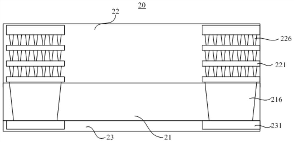
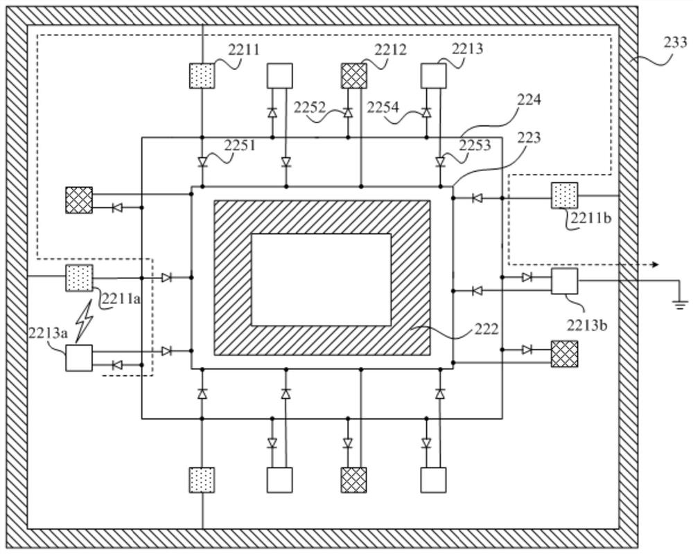
The present invention provides an electrostatic protection structure of an image sensor and an image sensor, the image sensor comprises: a substrate including a plurality of pixel regions; a first metal interconnection layer arranged on one side of the substrate, including a pixel peripheral circuit; and a second metal layer arranged on the other side of the substrate. The electrostatic protectionstructure comprises: a first electrostatic discharge protection circuit arranged on the first metal interconnection layer and a second electrostatic discharge protection circuit arranged on the second metal layer; wherein the impedance of the second electrostatic discharge protection circuit is smaller than that of the first electrostatic discharge protection circuit, and the second electrostaticdischarge protection circuit and the first electrostatic discharge protection circuit have at least one access point. The electrostatic protection structure can reduce the resistance of a leakage path and improve the electrostatic discharge performance of a chip under the premise of not increasing the chip area.
Need to check novelty before this filing date? Find Prior Art

Description

technical field

[0001] The invention relates to the technical field of image sensors, in particular to an electrostatic protection structure of an image sensor and an image sensor. Background technique

[0002] Back-illuminated (BSI) CMOS image sensors have many advantages over front-illuminated (FSI) CMOS image sensors, for example: the quantum efficiency of small-sized pixels can be greatly improved to adapt to the trend of high resolution; the thinning of the substrate makes the substrate The resistance is greatly increased, the propagation of noise in the substrate is suppressed, and the signal-to-noise ratio is improved. However, the increase in substrate resistance makes the chip's Electro-Static Discharge (ESD) performance more dependent on the ESD ring. To reduce the resistance of the ESD ring in a large-size chip requires a corresponding increase in the ESD ring. The width of the chip greatly increases the chip area and increases the manufacturing cost of the chip....

Examples

Embodiment Construction

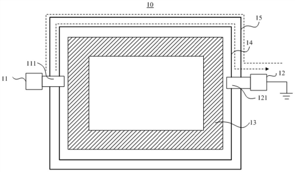
[0042] As mentioned in the background technology, there is a contradiction between the improvement of the electrostatic discharge performance of the existing back-illuminated image sensor and the development trend of chip miniaturization. For details, please refer to figure 1 , figure 1 is a schematic structural diagram of an electrostatic discharge protection circuit of the image sensor 10 .

[0043] In some embodiments, the image sensor 10 may be a CMOS image sensor, including a substrate, and a metal interconnection layer ( figure 1 It can be regarded as a top view of the metal interconnection layer), a plurality of pixel regions are arranged in the substrate, and a pixel peripheral circuit 13 and an electrostatic discharge protection circuit are arranged on the metal interconnection layer, wherein the pixel The peripheral circuit 13 is arranged around the pixel area in the substrate, and the electrostatic discharge protection circuit may include three leakage paths: the s...