
An electrostatic discharge protection circuit
A technology for electrostatic discharge protection and circuits, which is applied to circuits, electrical components, semiconductor devices, etc., and can solve problems such as easy triggering of latch-up effects
Patent Information
- Authority / Receiving Office
- CN · China
- Patent Type
- Patents(China)
- Current Assignee / Owner
- Publication Date
- 2020-01-31
Smart Images
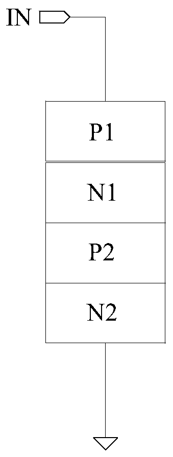
Figure 1 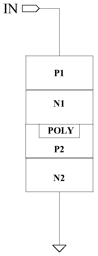
Figure 2
Abstract
Description
technical field
[0001] The invention belongs to the technical field of semiconductor integrated circuits, and in particular relates to an electrostatic discharge protection circuit. Background technique
[0002] Electrostatic discharge is a familiar and underappreciated source of damage to circuit boards and components during electronics assembly. It affects every manufacturer, no matter its size. While many people think they are producing products in an ESD-safe environment, the reality is that ESD-related damage continues to cost the electronics manufacturing industry worldwide billions of dollars annually.
[0003] A well-designed chip for electrostatic discharge should have a dedicated electrostatic discharge protection circuit on each input and output pin. The SCR (Silicon Controlled Rectifier) structure plays a very important role as a commonly used electrostatic discharge protection circuit. Common SCR (Silicon Controlled Silicon) structures such as figure 1 As ...
Examples
Embodiment Construction
[0009] In order to make the object, technical solution and advantages of the present invention clearer, the present invention will be further described in detail below in combination with specific embodiments and with reference to the accompanying drawings. It should be understood that these descriptions are exemplary only, and are not intended to limit the scope of the present invention. Also, in the following description, descriptions of well-known structures and techniques are omitted to avoid unnecessarily obscuring the concept of the present invention.
[0010] In order to solve the technical problem that the existing thyristor-type electrostatic discharge circuit easily triggers the latch-up effect, the present invention provides an electrostatic discharge protection circuit, such as figure 2 As shown, the circuit includes: the first P layer P1, the first N layer N1, the polysilicon layer POLY, the second P layer P2, and the second N layer N2, the first P layer P1, the ...