
Layout architecture with high-performance and high-density design
A layout and electrical connection technology, applied in the direction of electrical components, electrical solid devices, circuits, etc., can solve the problems of excessively long connecting lines, waste of layout area, and increased difficulty of winding, and achieve enhanced driving capabilities and high-performance design Effect
Patent Information
- Authority / Receiving Office
- CN · China
- Patent Type
- Applications(China)
- Current Assignee / Owner
- Publication Date
- 2008-02-13
- Estimated Expiration
- Not applicable · inactive patent
Smart Images
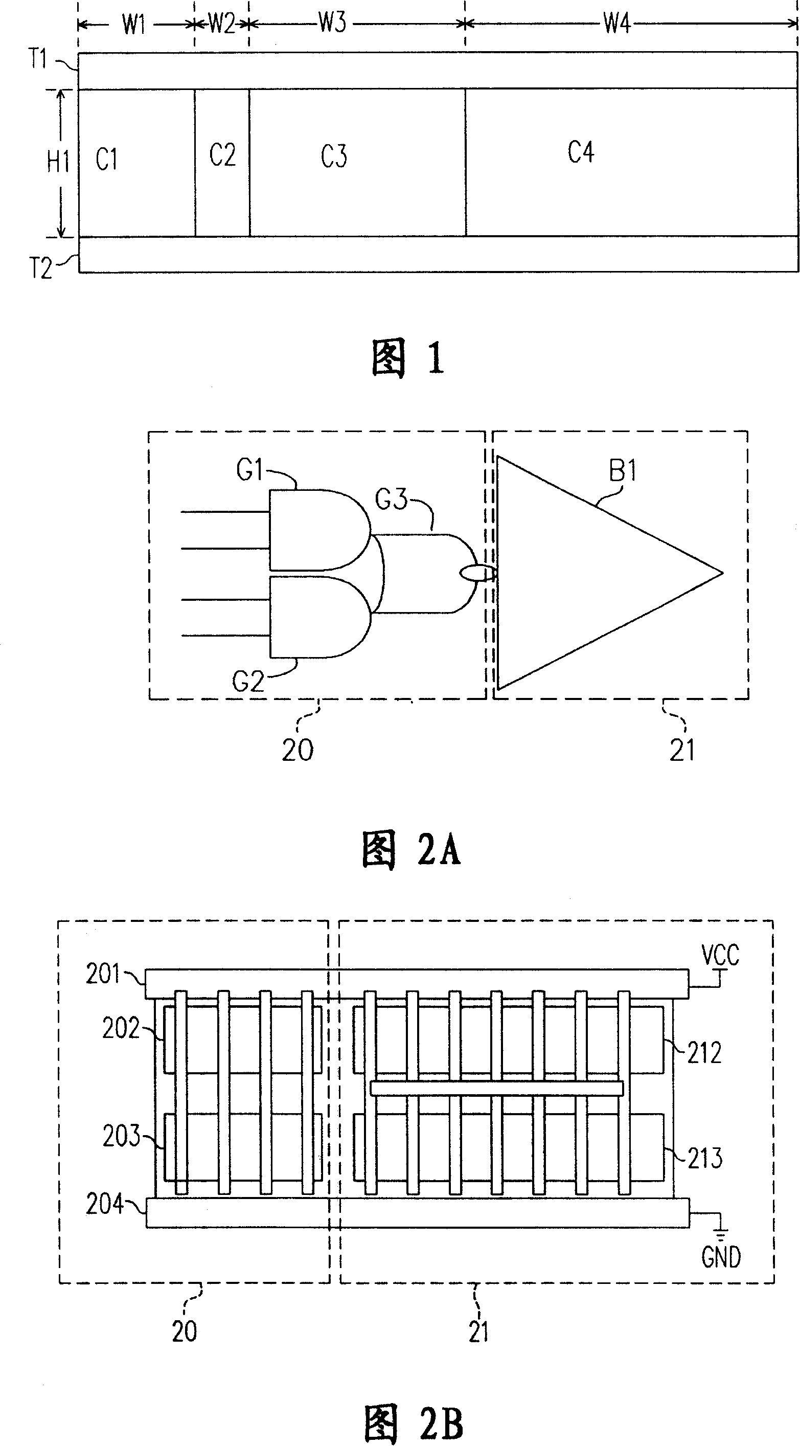
Figure 1 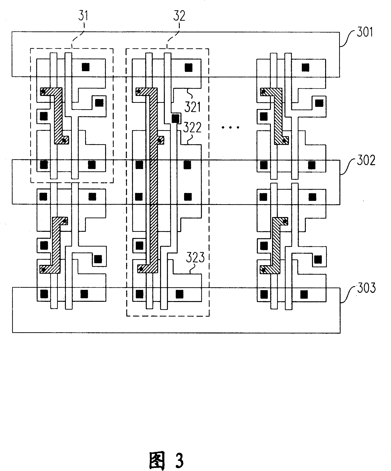
Figure 2 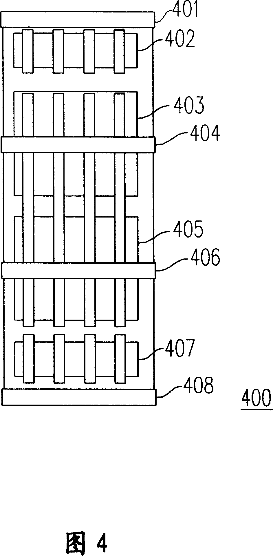
Figure 3
Abstract
Description
technical field
[0001] The present invention relates to a layout architecture, and more particularly to a layout architecture with high performance and high density design. Background technique
[0002] FIG. 1 is a layout diagram of an existing standard cell. The existing standard cells C1-C4 are located between the conductors T1 and T2, and can perform different functions such as amplifiers, adders, multipliers, and inverters, respectively. Therefore, the standard cells C1 to C4 are arranged with different widths W1 to W4 according to the complexity of the functions. In FIG. 1 , the width W4 is greater than the width W2 , so, under the same height H1 , the layout area of the standard cell C4 is larger than that of the standard cell C2 . Therefore, the standard cell C4 is suitable as a layout structure for a circuit with a relatively complex design or a circuit with a large driving current, and the standard cell C2 is suitable for a layout structure for a circuit with a ...
Examples
Embodiment Construction
[0032] FIG. 4 is a layout diagram of a high-performance and high-density layout architecture 400 according to an embodiment of the present invention. The standard unit 400 includes a base (not shown), and conductors 401, 404, 406, 408 and element regions 402, 403, 405, 407 are arranged on the base, the conductors 401, 406 have a voltage VCC, and the conductors 404, 408 have a voltage VCC GND.
[0033] The element area 402 is configured with a plurality of P-type metal oxide semiconductor (MOS) transistors for short, and the element area 402 is connected to the conductor 401 to obtain the voltage VCC, and the element area 402 is connected to the element area 403 . The element area 403 is configured with a plurality of N-type MOS transistors, the element area 403 is connected to the element area 402 and the element area 405 , and the element area 403 is located under the conductor 404 . The device area 403 can obtain the voltage GND through the connection conductor 404 . The e...