
Semiconductor device and method of bump formation
A manufacturing method and semiconductor technology, applied in semiconductor devices, semiconductor/solid-state device manufacturing, semiconductor/solid-state device components, etc., can solve problems such as inability to compress, reduce the conductivity of chips and carriers, etc.
Patent Information
- Authority / Receiving Office
- CN · China
- Patent Type
- Applications(China)
- Current Assignee / Owner
- Publication Date
- 2009-04-08
- Estimated Expiration
- Not applicable · inactive patent
Smart Images
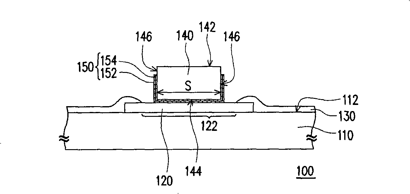
Figure 1 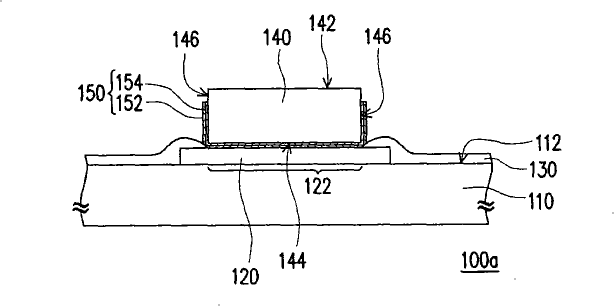
Figure 2 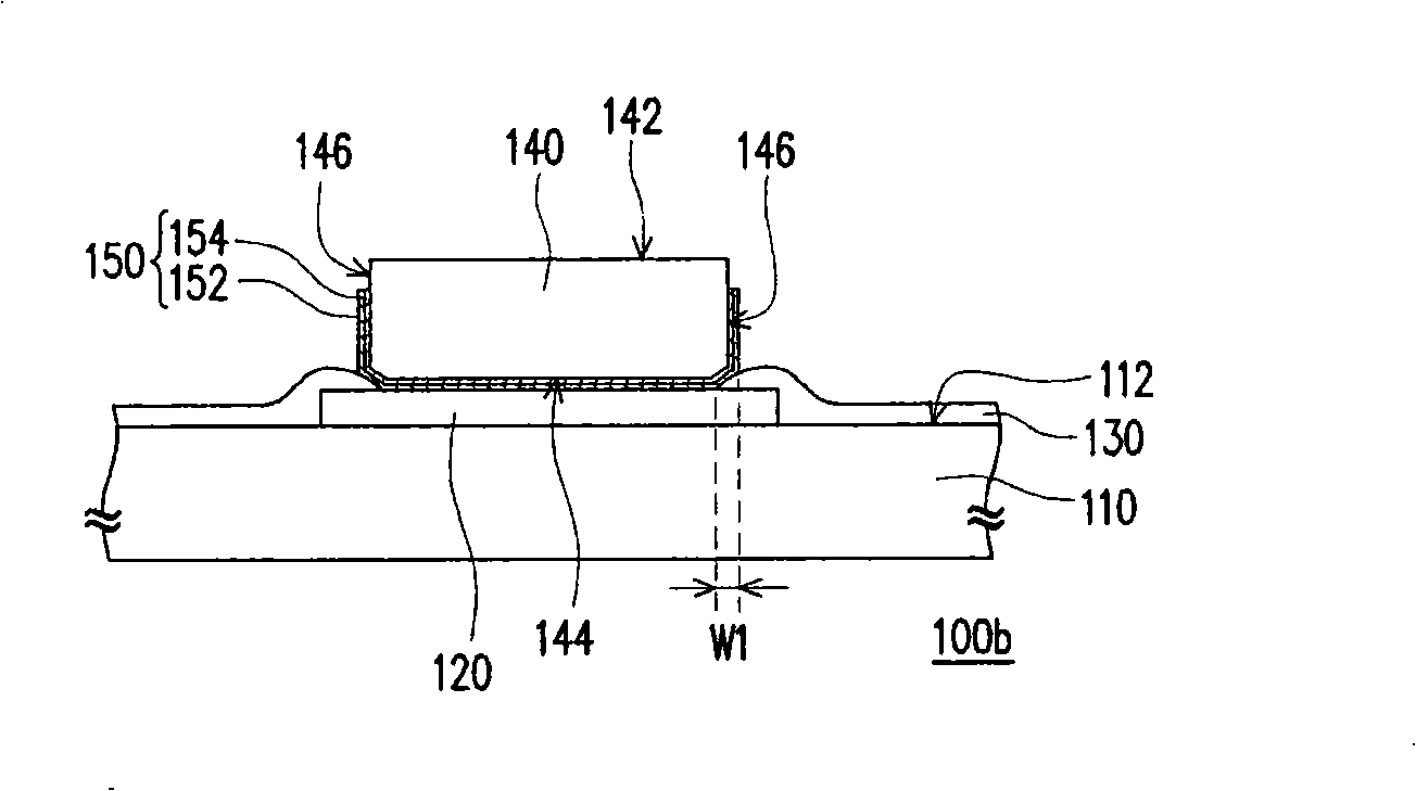
Figure 3
Abstract
Description
technical field
[0001] The invention relates to an electronic device and its technology, and in particular to a semiconductor element and a method for making bumps. Background technique
[0002] Flip-chip technology is a packaging technology often used in chip scale packaging (Chip Scale Packaging, CSP). Since the flip-chip technology adopts a planar array (Area Array) for the configuration of the pads on the chip, the packaging area can be reduced. In addition, since the flip-chip technology uses bumps to electrically connect the chip and the carrier, the signal transmission path can be shortened.
[0003] Generally, the chip surface is covered with a protective layer, which is present covering the chip surface and exposing the chip's aluminum pads. When the flip-chip technology is in progress, an under bump metal (UBM) layer will be formed on the protection layer and the pads first. Then, a photoresist layer is formed on the UBM layer, but the photoresist layer will exp...
Examples
Embodiment Construction
[0042] figure 1 is a schematic cross-sectional view of a semiconductor device according to an embodiment of the present invention. Please refer to figure 1 , the semiconductor device 100 of this embodiment includes a semiconductor substrate 110 , a plurality of pads 120 , a passivation layer 130 , a plurality of bumps 140 and a plurality of seed layers 150 . However, in figure 1 A pad 120 , a bump 140 and a seed layer 150 are represented in the figure. The semiconductor substrate 110 has an active surface 112 . Each pad 120 is disposed on the active surface 112 and is, for example, a metal pad. In the present embodiment, the semiconductor substrate 110 is, for example, a chip, which includes an integrated circuit electrically connected to the pads 120 . The passivation layer 130 is disposed on the active surface 112 and exposes the central portion 122 of each pad 120 . The protective layer is, for example, an insulating layer.
[0043] The seed layer 150 is disposed on ...