
Gold plated ZnO nano-bar array electrode and method for making same
A nanorod array and nanorod technology, applied in the field of electrochemistry, can solve the problems of difficult electrochemical electrodes, dissolution and corrosion, and no conductivity, etc., and achieve high sensitivity, extended service life, and stable chemical properties.
Patent Information
- Authority / Receiving Office
- CN · China
- Patent Type
- Patents(China)
- Current Assignee / Owner
- Publication Date
- 2012-05-23
- Estimated Expiration
- Not applicable · inactive patent
Smart Images
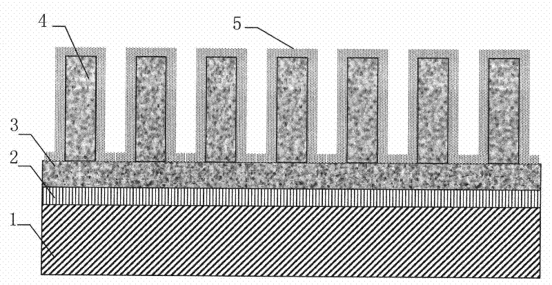
Figure 1 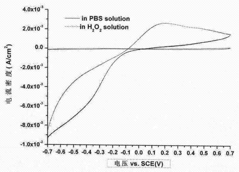
Figure 2 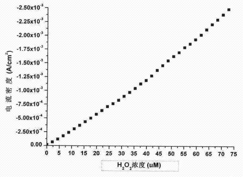
Figure 3
Abstract
Description
technical field
[0001] The invention relates to a gold-plated ZnO nanorod array electrode used in the field of electrochemistry, in particular to the structure and preparation method of the gold-plated ZnO nanorod array electrode. Background technique
[0002] Nanoelectrodes have excellent characteristics such as high mass transfer rate, low iR drop, and small time constant, and have been more and more widely studied and applied. The electrochemical properties of nano-array electrodes are not only related to the properties of nano-single electrodes, but also have some characteristics of their own, such as a much larger current intensity than nano-single electrodes, and a much higher Signal-to-noise ratio, etc. These characteristics make the preparation and application of nano-array electrodes better meet the practical requirements, and its research has gradually become one of the most active frontiers in the field of electrochemical research.
[0003] For one-dimensional n...
Examples
Embodiment Construction
[0017] Such as figure 1 , 4 As shown, the structure of the gold-plated ZnO nanorod array electrode is a silicon substrate 1, a silicon dioxide dielectric layer 2, a ZnO seed layer 3 and a ZnO nanorod array layer from bottom to top. The silicon dioxide dielectric layer 2 is located on the silicon substrate 1 , the ZnO seed layer 3 is located on the silicon dioxide dielectric layer 2 , and the ZnO nanorod array layer is located on the ZnO seed layer 3 . A gold layer 5 with the same thickness is plated on the surface of each ZnO nanorod 4 and the surface of the ZnO seed layer 3 in the ZnO nanorod array layer, the thickness of which is 150 nm.
[0018] The preparation method of the gold-plated ZnO nanorod array electrode mainly includes two steps, firstly the preparation of the ZnO nanorod 4 array, and finally the gold plating of the ZnO nanorod 4 array. The specific process is as follows. In the first step of the preparation of the ZnO seed layer 3, a p-type or n-type single cr...