
Method for producing semiconductor device
A technology for semiconductors and devices, applied in the field of manufacturing semiconductor devices, can solve the problems of destroying the gate oxide layer, different depths of etching, and inability to grind off silicides.
Patent Information
- Authority / Receiving Office
- CN · China
- Current Assignee / Owner
- Publication Date
- 2012-03-14
- Estimated Expiration
- Not applicable · inactive patent
Smart Images
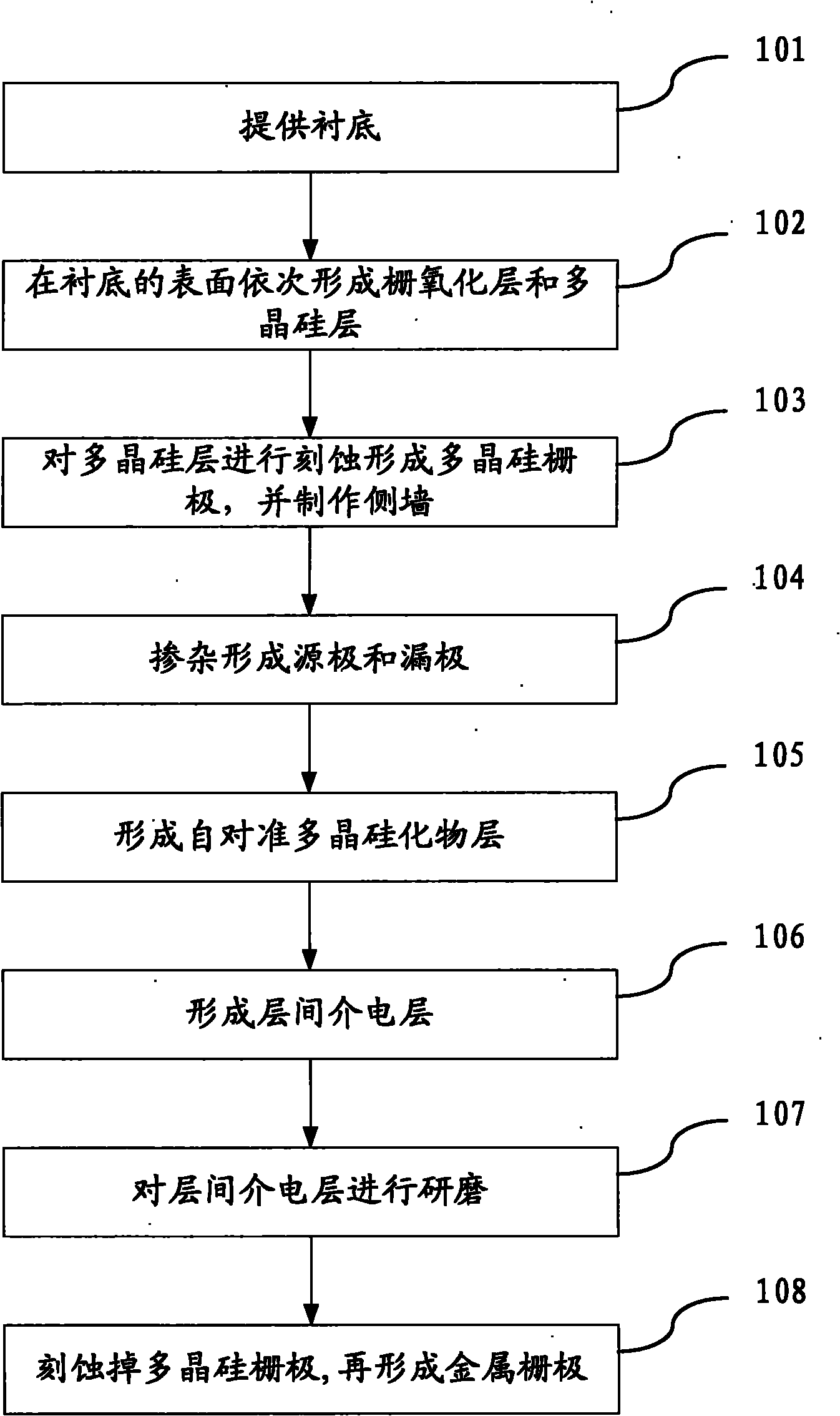
Figure 1 
Figure 2 
Figure 3
Abstract
Description
technical field
[0001] The present invention relates to semiconductor fabrication processes, and more particularly, the present invention relates to a method of fabricating a semiconductor device. Background technique
[0002] The gate usually has the smallest physical dimension in the semiconductor manufacturing process, and its width is usually the most critical critical dimension on the wafer, so the fabrication of the gate is the most critical step in the process in the semiconductor device manufacturing process.
[0003] Because polysilicon material has the advantages of high temperature resistance and the ability to prevent atoms doped by ion implantation from entering the channel region, polysilicon material is usually used to make the gate of the transistor when making a typical metal oxide semiconductor transistor. However, the polysilicon gate has some disadvantages. For example, the polysilicon gate has a relatively high resistance value, which is prone to depleti...
Examples
Embodiment Construction
[0032] In the following description, numerous specific details are given in order to provide a more thorough understanding of the present invention. It will be apparent, however, to one skilled in the art that the present invention may be practiced without one or more of these details. In other examples, some technical features known in the art are not described in order to avoid confusion with the present invention.
[0033] In order to provide a thorough understanding of the present invention, detailed steps will be set forth in the following description to illustrate how the present invention proposes a method of fabricating a semiconductor device. Obviously, the practice of the invention is not limited to specific details familiar to those skilled in the semiconductor arts. Preferred embodiments of the present invention are described in detail below, however, the present invention may have other embodiments besides these detailed descriptions.
[0034] Combine the follow...