
Method for forming pattern for transparent conductive layer
A technology of transparent conductive layer and transparent conductive film, applied in the direction of transparent dielectric, conductive layer on insulating carrier, circuit, etc., can solve problems such as difficult to remove accurately, difficulty, pattern short circuit, etc., and achieve excellent manufacturing efficiency and high manufacturing efficiency Effect
Patent Information
- Authority / Receiving Office
- CN · China
- Patent Type
- Applications(China)
- Current Assignee / Owner
- Publication Date
- 2012-07-11
- Estimated Expiration
- Not applicable · inactive patent
Smart Images

Figure 1 
Figure 2 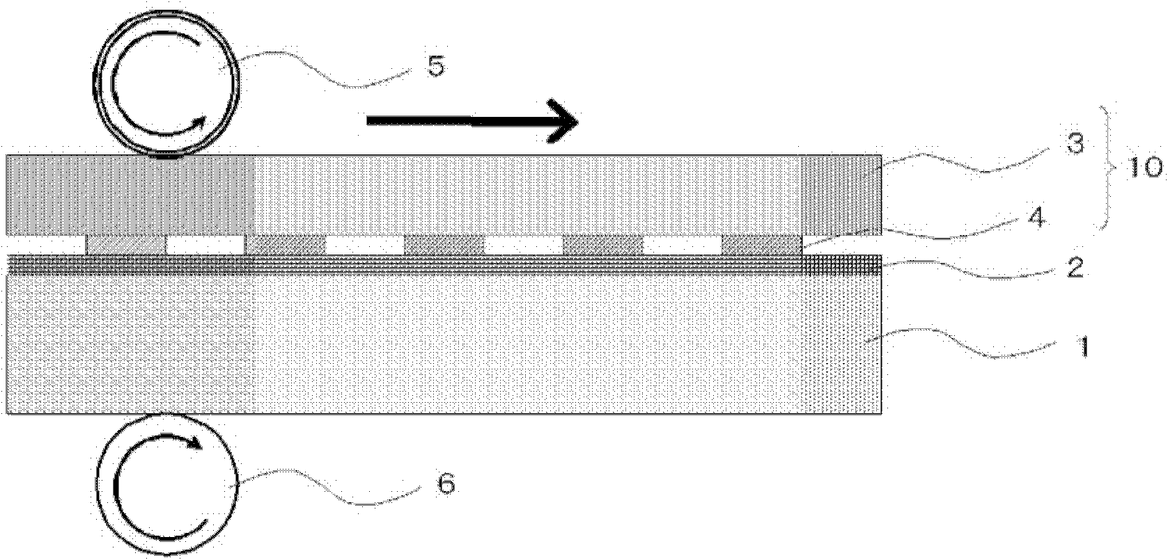
Figure 3
Abstract
Description
technical field
[0001] The invention relates to a method for forming a pattern of a transparent conductive layer on a substrate.
[0002] In more detail, the present invention relates to the use of a base formed of a fine conductive substance with a peelable transparent conductive layer and a layer formed with a negative patterned bonding region, more preferably a heat-sensitive adhesive layer. body, and use the partial peeling of the transparent conductive layer to form a transparent conductive layer pattern on the substrate. Background technique
[0003] In electronic devices utilizing light-emitting and light-receiving functions, various materials for forming transparent conductive layers and various transparent conductive layer films formed with transparent conductive layers on transparent substrates are mostly used as important functional components. Materials that pattern a transparent conductive layer to arrange a large number of conductive regions on a transparent s...
Examples
Embodiment
[0123] Hereinafter, the present invention will be described more specifically by citing examples in the production of a transparent conductive layer film for a touch panel when the transparent conductive substance is a nanowire, but the present invention is not limited to these examples.
[0124](a) (Synthesis of silver nanowires)
[0125] Silver nanowires are described in Y.Sun, B.Gates, B.Mayers, and Y.Xia, "Crystalline silver nanowires by soft solution processing", Nano letters, (2002), 2(2) 165-168 Nanowires synthesized by dissolving silver sulfate in ethylene glycol and reducing it in the presence of polyvinylpyrrolidone (PVP) as a mold followed by the method of using polyalcohol as a reducing agent. That is, in the present invention, nanowires synthesized by a modified polyol method as described in Cambrios Technologies Corporation US Provisional Application No. 60 / 815627 are used.
[0126] (b) (Formation of transparent conductive layer)
[0127] As metal nanowires to ...