
Tracking and boosting device and method for power factor correction circuit
A power factor correction and boosting device technology, which is applied in the direction of output power conversion device, DC power input conversion to DC power output, electrical components, etc., can solve the problems of being affected by temperature, voltage Vout1 is affected by temperature, etc., and achieve improvement efficiency effect
Patent Information
- Authority / Receiving Office
- CN · China
- Patent Type
- Patents(China)
- Current Assignee / Owner
- Publication Date
- 2016-01-06
Smart Images
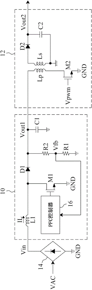
Figure 1 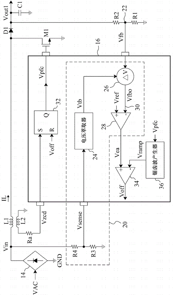
Figure 2 
Figure 3
Abstract
Description
technical field
[0001] The present invention relates to a power factor correction (PowerFactorCorrection; PFC) circuit, in particular to a tracking boost device and method for a power factor correction circuit. Background technique
[0002] Efficiency is an important issue for the power supply system of many high-end electronic products, such as notebook computers. For example refer to figure 1 In the power system shown, for high efficiency, the AC voltage VAC is rectified by the rectifier 14 and the main power supply voltage Vin is not directly used as the input voltage of the flyback voltage converter 12, but as the input of the power factor correction (PFC) circuit 10 The PFC circuit 10 generates a voltage Vout1 and then supplies it to the flyback voltage converter 12 as its input voltage. In the PFC circuit 10, the inductor L1 is connected between the rectifier 14 and the switch M1, the PFC controller 16 switches the switch M1 to control the charging and discharging of...
Examples
Embodiment Construction
[0057] refer to figure 2 , the power factor correction circuit includes the tracking boost device 20 according to the present invention to provide an error signal Vea related to its input voltage Vin, the sawtooth wave generator 36 generates the sawtooth wave signal Vramp according to the drive signal Vpfc of the switch M1, and the comparator 34 compares the error signal Vea and the sawtooth wave signal Vramp generate an off signal Voff, the auxiliary coil L2 induces the current IL of the inductor L1 to generate a sensing signal Vzcd, and the trigger 32 generates a driving signal Vpfc according to the sensing signal Vzcd and the off signal Voff to switch the switch M1 to input the input voltage Vin Converted to the output voltage Vout1, and the resistors R1 and R2 form a voltage divider to divide the output voltage Vout1 to generate a feedback voltage Vfb at the output feedback terminal 22 for the tracking boost device 20 . Since the error signal Vea is related to the input v...