
A surface plasmon waveguide with mis capacitance structure
A surface plasmon and waveguide technology, applied in the direction of light guides, optical components, nanotechnology, etc., can solve the problems of unfavorable device integration, reduce the thickness of the metal layer, limit the mode field, etc., achieve the enhancement of the local characteristics of the light field, and improve the integration The effect of degree and efficient regulation
Patent Information
- Authority / Receiving Office
- CN · China
- Patent Type
- Patents(China)
- Current Assignee / Owner
- Publication Date
- 2016-07-06
- Estimated Expiration
- Not applicable · inactive patent
Smart Images
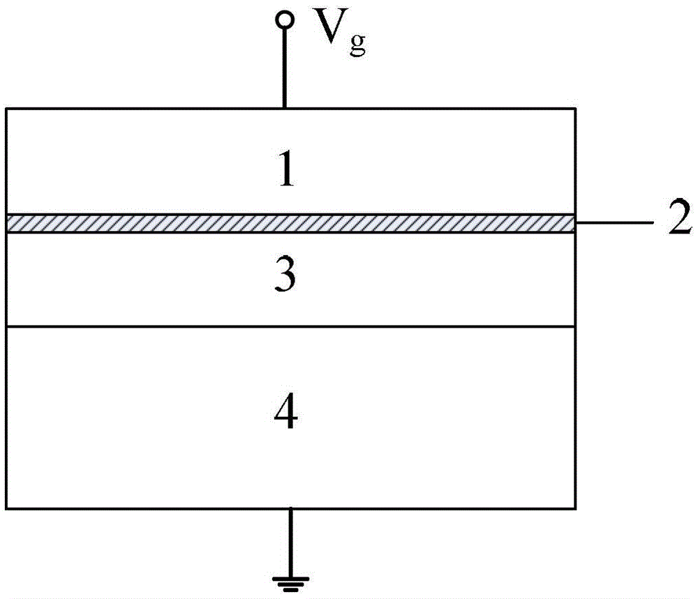
Figure 1 
Figure 2 
Figure 3
Abstract
Description
technical field
[0001] The invention relates to a Surface Plasmon Polariton (SPP) waveguide structure and device with a metal-insulator-semiconductor (Mental-Insulator-Semiconductor, MIS) capacitance structure, which utilizes a semiconductor layer and an insulating material under the action of an applied voltage The change of the complex dielectric function and its distribution of semiconductor materials near the layer interface can realize the switch of SPP wave transmission and the control of SPP field strength, and has potential applications in photonic integration, nonlinear optics and other fields. Background technique
[0002] The SPP wave is an electromagnetic wave guided at the interface between a conductor and a medium, which originates from the collective oscillation of free charges near the surface of the conductor caused by the excitation of an external electromagnetic field. The local enhancement effect brought by the unique generation mechanism of SPP waves and...
Examples
Embodiment 1
[0035] The SPP waveguide of embodiment 1.MIS capacitor structure
[0036] see figure 1 , the SPP waveguide is composed of a metal layer 1 , an insulating material layer 2 , a doped semiconductor layer 3 and a substrate 4 arranged from top to bottom.
[0037] The metal layer 1 may be a silver (Ag) layer.
[0038] The insulating material layer 2 can adopt zirconium dioxide (ZrO 2 )layer.
[0039] The doped semiconductor layer 3 can use In which is lattice-matched with InP. 0.53 Ga 0.47 As semiconductor layer. The thickness of the doped semiconductor layer should be at least greater than 35nm to ensure that positive and negative ε can appear near the interface of the semiconductor layer r interface.
[0040] The substrate 4 may be an InP substrate.
[0041] The selection of the material and thickness of the insulating material layer has a decisive effect on the realization of the device characteristics. When the dielectric constant of the insulating material is low, the c...
Embodiment 2
[0042] Example 2. SPP waveguide with MIS capacitor structure for 1550nm optical communication band (photon energy is about 0.8eV)
[0043] see figure 1 , the SPP waveguide is composed of a metal layer 1, an insulating material layer 2, a doped semiconductor layer 3 and a substrate 4 arranged from top to bottom, wherein:
[0044] The metal layer 1 may be silver (Ag) with a thickness of 100nm.
[0045] The insulating material layer 2 can adopt zirconium dioxide (ZrO2) with a thickness of 10 nm. 2 ).
[0046] The doped semiconductor layer 3 can use In which is lattice-matched with InP. 0.53 Ga 0.47 As, the thickness is 50nm, the doping concentration is 1×10 19 cm -3 , using N-type doping. where In 0.53 Ga 0.47 The selection of As doping concentration takes into account the intrinsic In 0.53 Ga 0.47 As material has the problem of intrinsic absorption in the optical communication window (~0.8eV). In 0.53 Ga 0.47 The direct bandgap of As is 0.74eV, and the Fermi level ...