
A method for forming ohmic contact of (100) oriented n-type single crystal diamond electrode
A single crystal diamond, ohmic contact technology, applied in the direction of circuits, electrical components, semiconductor devices, etc., can solve the problems of high contact resistivity, difficult ohmic preparation, etc., to achieve lower specific contact resistivity, lower requirements, and good ohmic contact Effect
Patent Information
- Authority / Receiving Office
- CN · China
- Patent Type
- Patents(China)
- Current Assignee / Owner
- Publication Date
- 2020-11-17
Smart Images
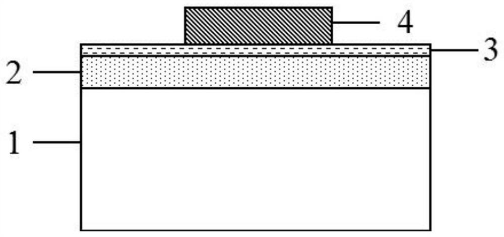
Figure 1 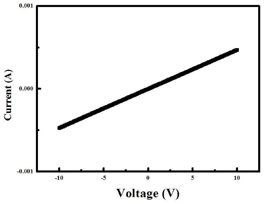
Figure 2
Abstract
Description
technical field
[0001] The invention belongs to the technical field of electronic engineering, and in particular relates to a (100) orientation n-type single crystal diamond electrode ohmic contact forming method. Background technique
[0002] The n-type doping technology of diamond semiconductors limits its wide application in electronic devices. Japan's Material and Materials Research Institute used microwave plasma chemical vapor deposition (MPCVD) to successfully achieve n-type doping of diamond single crystal thin films on the surface of single crystal diamond (111) using phosphorus atoms. On this basis, they quickly carried out the application of diamond p-n junction and p-i-n junction diodes in the field of light-emitting devices and power electronic devices. However, the (111) plane has the problem of difficult mechanical polishing, and its metal / diamond contact interface properties and the photoelectric properties of the film are worse than that of the (100) plane....
Examples
Embodiment 1
[0031] Such as figure 1 , a (100) oriented n-type single crystal diamond electrode ohmic contact forming method, (100) oriented n-type single crystal diamond 1 is a self-supporting body material with a size of 3 × 3 × 0.3mm 3 , with a surface roughness of 1 nm. A 10nm-thick n-type diamond epitaxial thin layer 2 was epitaxially grown on its surface by MPCVD, and the growth conditions were: air pressure 100 Torr, gas flow rate 500 sccm, CH 4 / H 2 = 1%, PH 3 / CH 4 =0.1%, and the substrate temperature was 900°C. After the growth, the sample was placed in a 1:1 mixture of sulfuric acid and nitric acid, heated at 250 °C for 1 h to convert the surface hydrogen terminals into oxygen terminals, and annealed at 900 °C for 5 min to obtain a highly conductive diamond surface 3. Through photolithography, magnetron sputtering, and lift-off processes, W metal electrodes 4 are prepared on the high-conductivity diamond surface 3, and then annealed at 400° C. for 10 minutes in an argon atm...
Embodiment 2
[0033] Such as figure 1 , a (100) orientation n-type single crystal diamond electrode ohmic contact forming method, (100) orientation n-type single crystal diamond 1 is a single crystal thin film, the size is 10 × 10 × 0.001mm 3 , with a surface roughness of 2nm. The n-type diamond epitaxial thin layer 2 with a thickness of 100nm is epitaxially grown on its surface by MPCVD method, and the growth conditions are: air pressure 100Torr, gas flow rate 500sccm, CH 4 / H 2 = 1%, PH 3 / CH 4 = 1%, and the substrate temperature was 900°C. After the growth, the surface hydrogen terminals were transformed into oxygen terminals by ultraviolet ozone treatment, and annealed at 1100° C. for 5 minutes to obtain a highly conductive diamond surface 3 . Prepare Ti / Pt / Au metal electrodes 4 on the high-conductivity diamond surface 3 by photolithography, magnetron sputtering, and lift-off processes, and then anneal at 700° C. for 20 minutes in an argon atmosphere to form ohmic contacts.
Embodiment 3
[0035] Such as figure 1 , a (100) orientation n-type single crystal diamond electrode ohmic contact forming method, (100) orientation n-type single crystal diamond 1 is a self-supporting body material, the size is 5 × 5 × 0.5mm 3 , with a surface roughness of 2nm. A 50nm-thick n-type diamond epitaxial thin layer 2 was epitaxially grown on its surface by MPCVD method, and the growth conditions were: air pressure 100 Torr, gas flow rate 500 sccm, CH 4 / H 2 = 1%, PH 3 / CH 4=0.5%, and the substrate temperature was 900°C. After the growth, the sample was placed in a 1:1 mixture of sulfuric acid and nitric acid, heated at 250 °C for 1 h to convert the surface hydrogen terminals into oxygen terminals, and annealed at 1000 °C for 10 min to obtain a highly conductive diamond surface 3. Prepare Ti / Au metal electrodes 4 on the highly conductive diamond surface 3 by photolithography, magnetron sputtering, and lift-off processes, and then anneal at 550°C for 20 minutes in an argon atm...