
Method for improving ohm of p-type gallium nitride
A technology of gallium nitride and gallium nitride layer, which is applied in the field of semiconductor material growth and device preparation, can solve the problems of difficult to achieve high-quality p-type gallium nitride ohmic contact and low hole concentration, achieve low ohmic contact, simplify Process, the effect of realizing ohmic contact
Patent Information
- Authority / Receiving Office
- CN · China
- Patent Type
- Applications(China)
- Current Assignee / Owner
- Publication Date
- 2020-07-24
- Estimated Expiration
- Not applicable · inactive patent
Smart Images
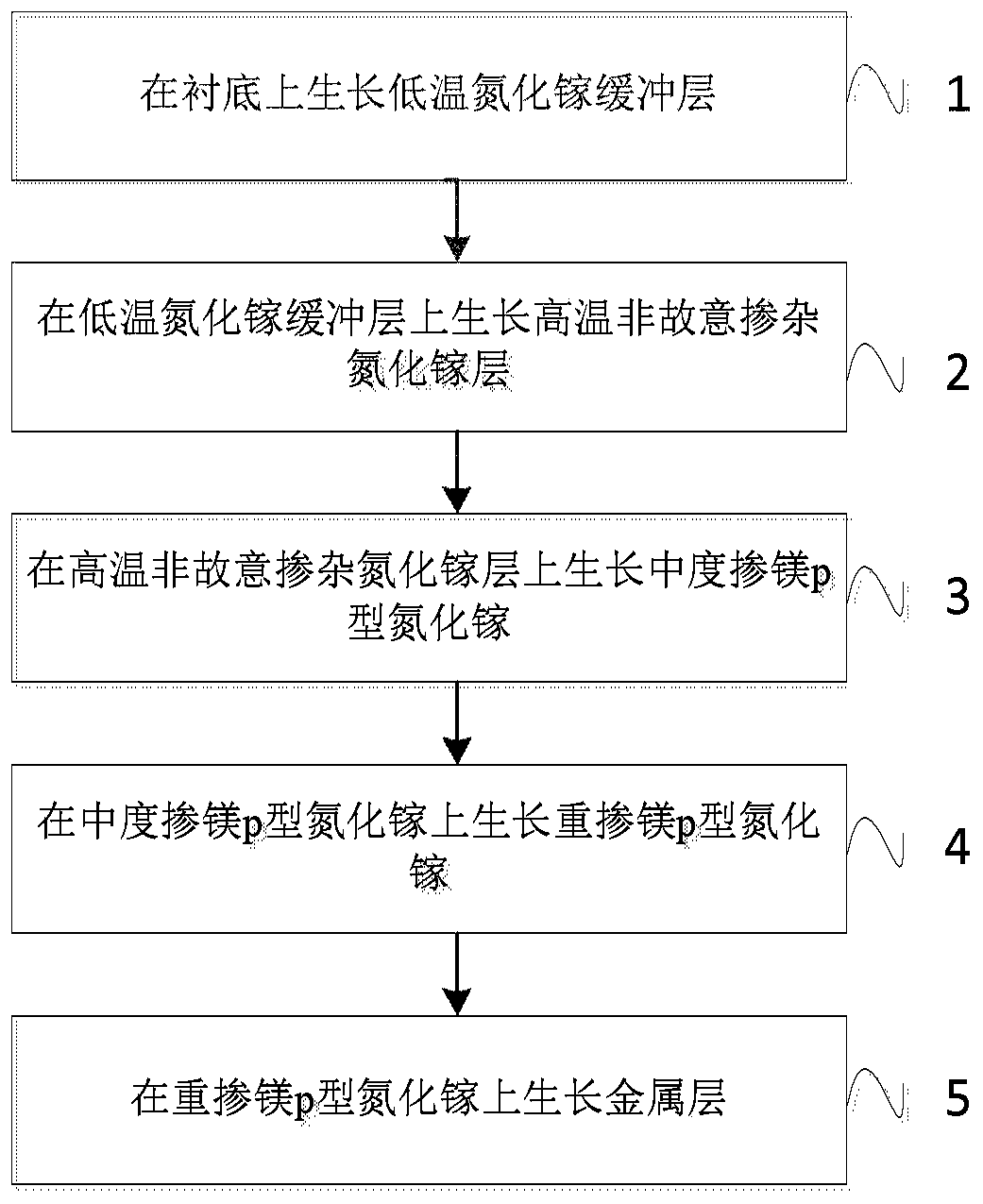
Figure 1 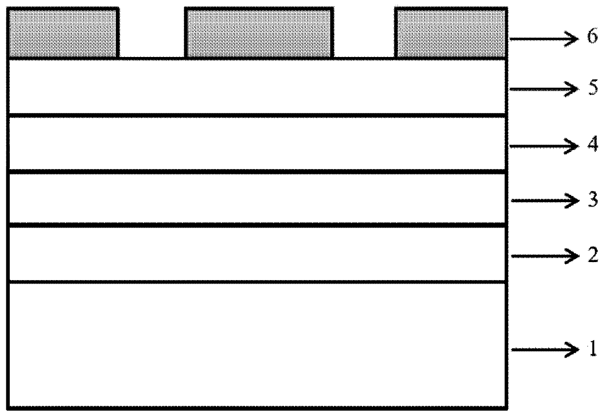
Figure 2 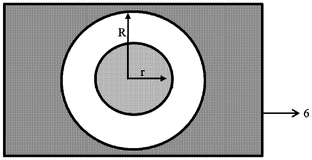
Figure 3
Abstract
Description
technical field
[0001] The disclosure relates to the field of semiconductor material growth and device preparation, and in particular to a method for improving p-type gallium nitride ohms. Background technique
[0002] Gallium nitride material systems have shown excellent performance in the fields of optoelectronic and microelectronic devices such as solid-state light-emitting diodes, blue / green lasers, high electron mobility transistors and solar cells. Among them, gallium nitride-based lasers have the advantages of adjustable wavelength, high efficiency, small size, and controllable time and space, and have important application value in the fields of submarine communication, laser mine detection, laser display, laser micro-projection, and laser lighting.
[0003] How to obtain a good p-type GaN ohmic contact is an important basis for the wide application of GaN-based devices. For example, the working voltage of GaN-based lasers is directly related to the p-type ohmic cont...
Examples
Embodiment
[0048] Step S1: Infuse ammonia gas, and turn on the gallium source. A 50nm low-temperature gallium nitride buffer layer 2 is grown on a sapphire substrate 1 by metalorganic chemical vapor deposition method, and the growth temperature is 550°C.
[0049] Step S2: growing a high-temperature unintentionally doped gallium nitride layer 3 of 1000 nm on the low-temperature gallium nitride buffer layer 2 by using metalorganic chemical vapor deposition, and the growth temperature is 1100° C.
[0050] Step S3: growing a moderately magnesium-doped p-type gallium nitride layer 4 on the unintentionally doped gallium nitride layer, the thickness of which is 500 nm, wherein the concentration of magnesium acceptor impurities is about 1×10 19 em -3 .
[0051] Step S4: grow a heavily magnesium-doped p-type gallium nitride layer 5 with a thickness of about 20 nm on the moderately magnesium-doped p-type gallium nitride layer 4, and control the carbon impurity concentration of the layer by adjus...