
Group-III nitride p-type ohmic electrode structure with low contact resistance
A technology of low contact resistance and electrode structure, applied in the direction of circuits, electrical components, laser components, etc., can solve problems such as low solid solubility, limited tunneling effect, and limited concentration, achieve high tunneling probability characteristics, and improve ohm Contact characteristics and the effect of reducing contact resistivity
Patent Information
- Authority / Receiving Office
- CN · China
- Patent Type
- Patents(China)
- Current Assignee / Owner
- Publication Date
- 2020-12-22
Smart Images
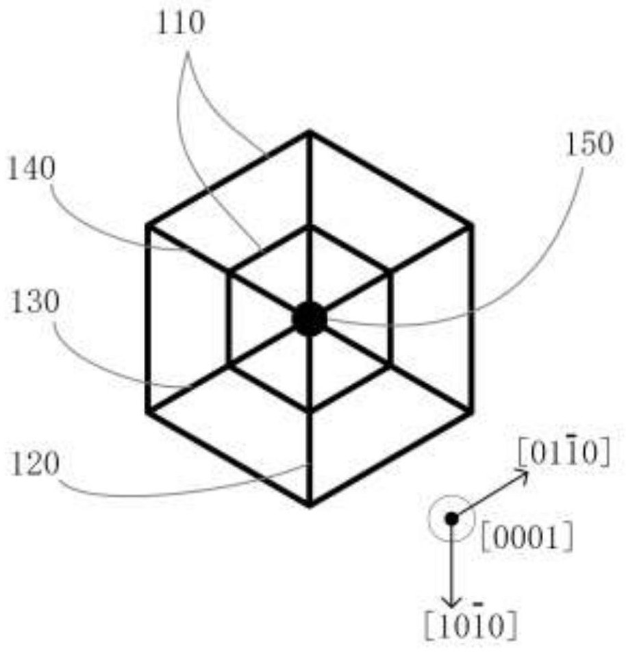
Figure 1 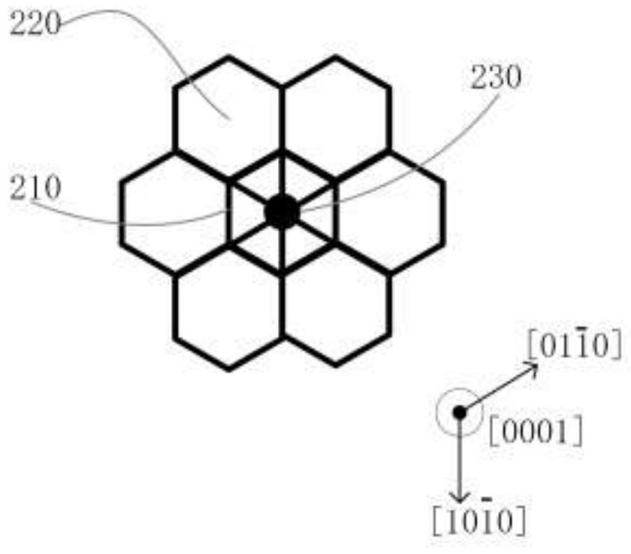
Figure 2 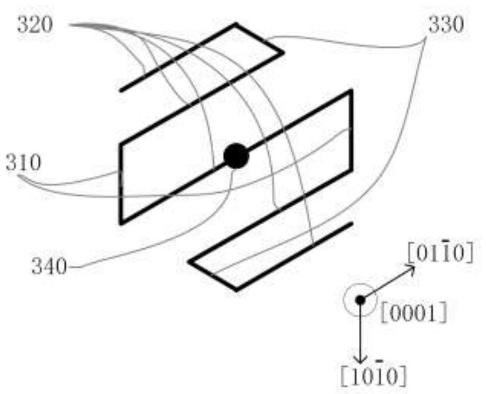
Figure 3
Abstract
Description
technical field
[0001] The invention relates to the technical field of semiconductor devices, in particular to a group III nitride p-type ohmic electrode structure with low contact resistance. Background technique
[0002] Compound semiconductor gallium nitride (GaN)-based materials have excellent chemical and chemical properties such as wide direct band gap, strong atomic bond, high thermal conductivity, good chemical stability, strong radiation resistance, and fast electron saturation migration speed. physical properties. In particular, by adjusting the composition of the GaN-based material ternary compounds AlGaN, AlInN and InGaN, and the quaternary compound AlInGaN, the band gap of the material can be changed, the energy band can be tailored, and the corresponding wavelength of the band gap can be changed from infrared to deep ultraviolet. continuous change. The advantages of these material properties make the III-nitrides represented by GaN have received extensive att...
Examples
Embodiment Construction
[0022] The present invention will be described in further detail below in conjunction with accompanying drawing:
[0023] see figure 1 As shown, as the first embodiment of the present invention, the electrode structure is a regular hexagonal spider web shape, including two concentric regular hexagonal line bodies 110, connecting three pairs of opposite corners of the regular hexagonal line bodies The three positive diagonal lines (120, 130, 140), the welding wire electrode part 150 located at the geometric center of the electrode structure or the intersection of any electrode pattern line body, there are two groups of the three groups of opposite sides of the regular hexagonal line body They are respectively consistent with the first crystal orientation and the second crystal orientation of the III-group nitride, and the remaining group is consistent with the equivalent crystal orientation of the first crystal orientation and the second crystal orientation of the III-group ni...