
Lateral double diffused field effect transistor, manufacturing method, chip and circuit
A technology of field effect transistors and lateral double diffusion, which is applied in the direction of circuits, semiconductor/solid-state device manufacturing, electrical components, etc., can solve the problems of driving ability and speed difference, and achieve increased speed, improved carrier mobility, and weakened band The effect of scattering
Patent Information
- Authority / Receiving Office
- CN · China
- Patent Type
- Patents(China)
- Current Assignee / Owner
- Publication Date
- 2022-05-31
Smart Images
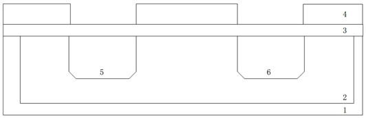
Figure 1 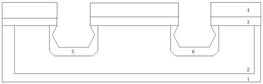
Figure 2 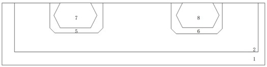
Figure 3
Abstract
Description
Lateral double diffusion field effect transistor, fabrication method, chip and circuit technical field The present invention relates to semiconductor technology field, particularly, relate to a kind of lateral double diffusion field effect transistor fabrication method Method, a lateral double diffusion field effect transistor, a chip and a circuit. Background technique Lateral Double Diffused Field Effect Transistor (Lateral Double-Diffused MOSFET, LDMOS) is used as a kind of Lateral power devices, whose electrodes are all located on the surface of the device, are easily connected to low-voltage signal circuits and other The monolithic integration of the device also has the advantages of high withstand voltage, large gain, good linearity, high efficiency, and good broadband matching performance. Nowadays, it has been widely used in power integrated circuits, especially low-power and high-frequency circuits. In the prior art, the lateral double diffusion field effe...
Examples
Embodiment Construction
[0031] The specific implementation of the embodiments of the present invention will be described in detail below in conjunction with the accompanying drawings. It should be understood that this
[0034] The present invention will be described in detail below with reference to the accompanying drawings and in conjunction with the embodiments.
[0038] A first drain 10 is formed in the first tensile strain region 7, a second drain 11 is formed in the second tensile strain region 8, and a P-type body is formed.
[0039] Through the lateral double diffusion field effect transistor of the embodiment of the present invention, a strained material is embedded in the drift region to form
[0040] Further, the first tensile strain region 7 and the second tensile strain region 8 are hexagonal structures.
[0042] Further, the first tensile strain region 7 and the second tensile strain region 8 include silicon carbide.
[0044] Further, the first tensile strain region 7 and the second tensile...