
Method for improving erasing speed of SONOS (Silicon Oxide Nitride Oxide Silicon) by utilizing strained silicon technology
A technology of erasing and writing speed and strained silicon, which is applied in the manufacturing of electrical components, electric solid-state devices, semiconductor/solid-state devices, etc., can solve the problem of low hot electron injection programming efficiency, etc., to improve programming efficiency and speed, energy valley scattering probability The effect of reducing, reducing the effective mass
Patent Information
- Authority / Receiving Office
- CN · China
- Patent Type
- Patents(China)
- Current Assignee / Owner
- Publication Date
- 2014-07-02
Smart Images
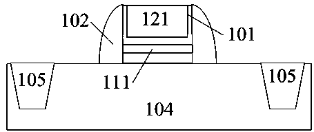
Figure 1 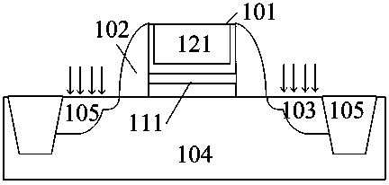
Figure 2 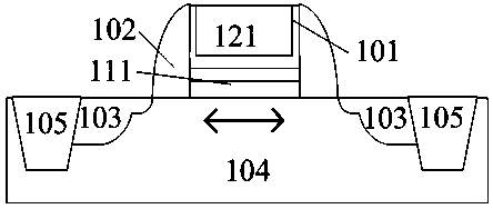
Figure 3
Abstract
Description
technical field
[0001] The invention relates to a silicon-silicon oxide-silicon nitride-silicon oxide-silicon (SONOS) memory, in particular to a method for improving the erasing and writing speed of the SONOS by utilizing strained silicon technology. Background technique
[0002] The basic working principle of non-volatile semiconductor memory is to store charge in the gate dielectric of a MOSFET. Devices in which charges are stored in discrete trapping centers in a suitable dielectric layer are called charge-trapping devices. The most common of these devices is silicon-silicon oxide-nitride-silicon oxide-silicon (SONOS) memory.
[0003] The main two storage mechanisms for storing data in flash memory cells are channel hot electron (CHE) injection and F-N tunneling. Channel hot electron injection is considered to be quite reliable after long-term cycling because it does not place significant stress on the tunnel oxide. But the disadvantage of CHE is that the programming e...
Examples
Embodiment Construction
[0024] The present invention will be described in further detail below in conjunction with the accompanying drawings and specific embodiments. The specific embodiments described here are only used to explain the present invention, and are not used to limit the protection scope of the present invention.
[0025] combined reference figure 1 and figure 2 , revealing the method of the present invention to improve the erasing and writing speed of SONOS by utilizing the strained silicon technology, figure 1 In the process, after forming the sidewall 102 of the gate 101 on the P-type substrate 104 with several shallow trench isolation regions 105 formed, the following steps are also included:
[0026] Step 1, precipitation barrier layer ( figure 1 not shown) covering the transistor;
[0027] Step 2, etch and remove the barrier layer covering the NMOS region to expose the NMOS region. In this step, first spin-coat photoresist on the barrier layer, and then perform photolithograph...