
Diamond material ohmic contact electrode and its preparation method and application
An ohmic contact electrode and diamond technology, which is applied in the manufacturing of circuits, electrical components, semiconductor/solid-state devices, etc., can solve the problems of poor thermal stability, poor adhesion between gold and diamond materials, and increased resistance, and reduce specific contact resistivity. , Improve electrical properties, increase the effect of adhesion
Patent Information
- Authority / Receiving Office
- CN · China
- Patent Type
- Patents(China)
- Current Assignee / Owner
- Publication Date
- 2018-05-04
Smart Images
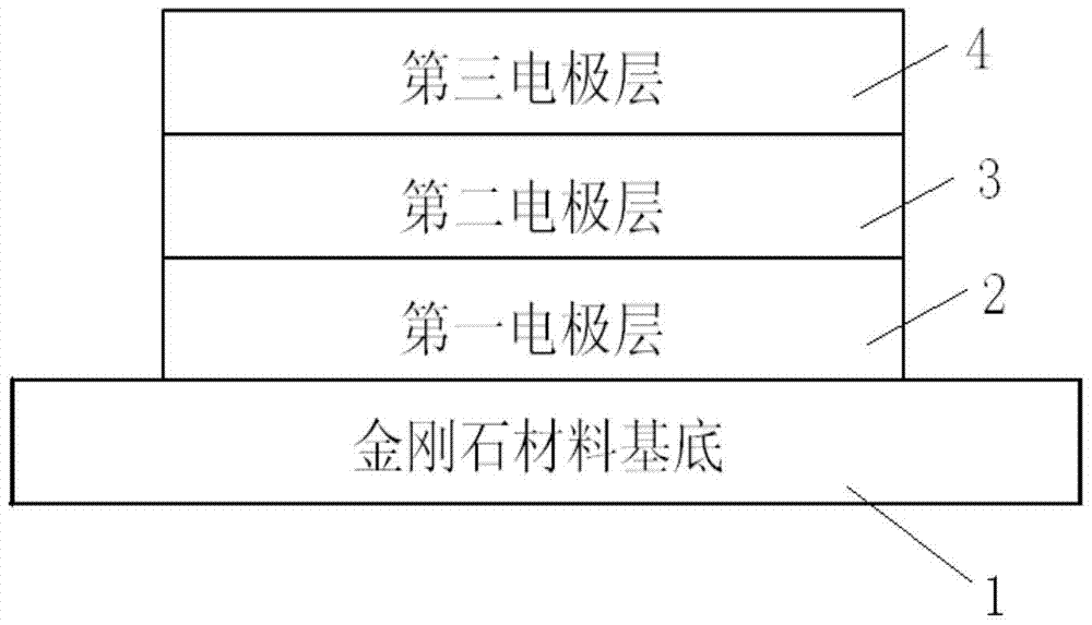
Figure 1 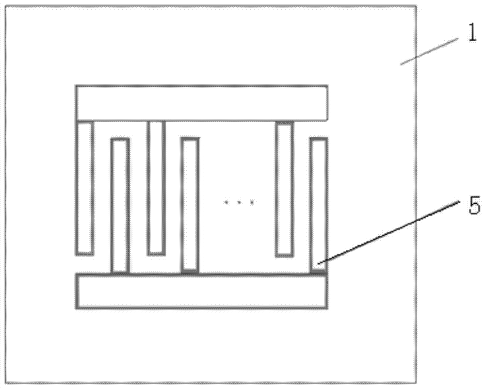
Figure 2 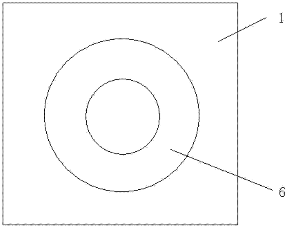
Figure 3
Abstract
Description
technical field
[0001] The invention belongs to the technical field of diamond chemical vapor deposition, and relates to a diamond material ohmic contact electrode and a preparation method and application thereof. Background technique
[0002] Semiconductor single crystal materials have gone through four generations of development. The first generation of Si and Ge semiconductors brought mankind into the information age, and at the same time drove the intelligence and informatization of electronic systems. The second-generation semiconductors (GaAs, InP, MCT, etc.) have brought us optoelectronic devices, power electronic devices, radio frequency electronic devices, and space radiation-resistant devices, etc., which have triggered revolutions in information fields such as wireless communications and optical communications. The third-generation wide-bandgap semiconductors (GaN, SiC) can partially meet the requirements of the new generation of electronic systems for semiconduc...
Examples
Embodiment 1
[0055] A method for preparing a diamond material ohmic contact electrode comprises the following steps:
[0056] 1) Use microwave plasma chemical vapor deposition (MPCVD) technology to deposit a layer of high-quality single crystal diamond epitaxial film of about 1 micron on the cleaned high-temperature and high-pressure (HPHT) diamond material substrate, for use;
[0057] 2) Use a mixed acid solution (1:1) of sulfuric acid and nitric acid to clean the deposited epitaxial film in a water bath at 250°C for about 1 hour to remove the carbon elements in the non-diamond phase on the surface;
[0058] 3) Use MPCVD equipment to hydrogenate the diamond epitaxial film, the plasma power is about 1000W, and the processing time is about 5 minutes;
[0059] 4) Use acetone, isopropanol, and deionized water to ultrasonically clean the sample, and dry it;
[0060] 5) Spin-coat a layer of AZ5214 photoresist on the surface of the sample, bake the spin-coated photoresist-coated single crystal ...
Embodiment 2
[0066] A method for preparing a diamond material ohmic contact electrode comprises the following steps:
[0067] 1) Deposit a layer of high-quality single-crystal diamond epitaxial film of about 1 micron on the cleaned high-temperature and high-pressure (HPHT) diamond substrate by using hot filament chemical vapor deposition (HFCVD) technology, for use;
[0068] 2) Use a mixed acid solution (1:1) of sulfuric acid and nitric acid to clean the deposited epitaxial film in a water bath at 250°C for about 1 hour to remove the carbon elements in the non-diamond phase on the surface;
[0069] 3) Use MPCVD equipment to hydrogenate the diamond epitaxial film, the plasma power is about 1000W, and the processing time is about 5 minutes;
[0070] 4) Use acetone, isopropanol, and deionized water to ultrasonically clean the sample, and dry it;
[0071] 5) Spin-coat a layer of AZ5214 photoresist on the surface of the sample, bake the spin-coated photoresist-coated single crystal diamond sam...
Embodiment 3
[0076] A method for preparing a diamond material ohmic contact electrode comprises the following steps:
[0077] 1) Use a mixed acid solution (1:1) of sulfuric acid and nitric acid to clean the high-temperature and high-pressure (HPHT) diamond substrate in a water bath at 250°C for about 1 hour to remove the carbon element of the non-diamond phase on the surface;
[0078] 2) Use MPCVD equipment to hydrogenate the diamond substrate, the plasma power is about 1000W, and the processing time is about 5 minutes;
[0079] 3) Use acetone, isopropanol, and deionized water to ultrasonically clean the sample, and dry it;
[0080] 4) Spin-coat a layer of AZ5214 photoresist on the surface of the sample, bake the spin-coated photoresist-coated single crystal diamond sample at 95°C for 90 seconds, use the designed mask plate for UV lithography exposure for 6.5s, and develop 45s to remove the exposed photoresist, leaving the design pattern;
[0081] 5) Place the photolithographic sample in...