

A transistor, a pixel unit, an array substrate and a display device
A technology for array substrates and transistors, which is applied in the fields of array substrates and display devices, pixel units, and transistors, and can solve problems such as thin photoresist thickness, affecting TFT performance, and changing TFT width-to-length ratio
Patent Information
- Authority / Receiving Office
- CN · China
- Patent Type
- Patents(China)
- Current Assignee / Owner
- Publication Date
- 2016-01-27
Smart Images
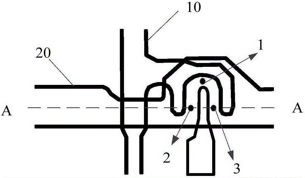
Figure 1 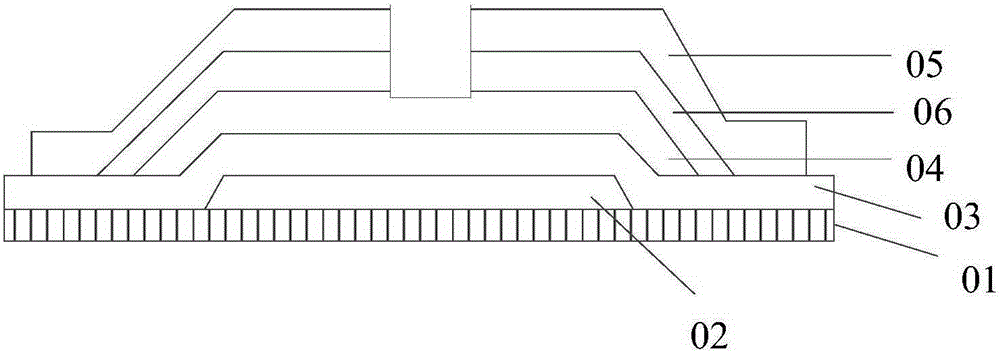
Figure 2 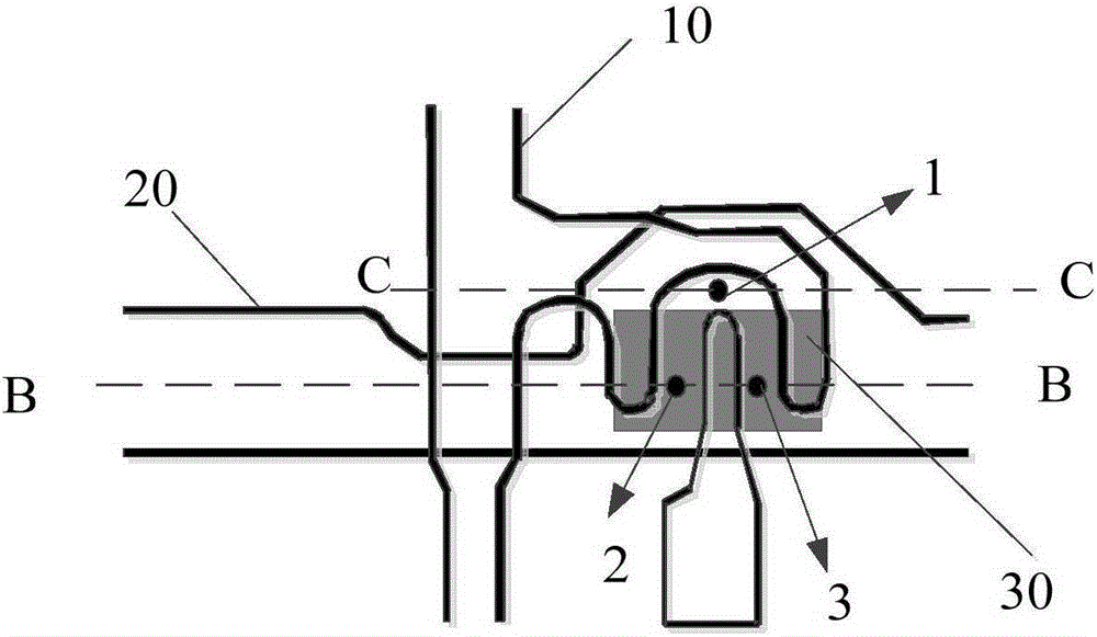
Figure 3
Abstract
Description
technical field
[0001] The invention relates to the field of display panel manufacturing, in particular to a transistor, a pixel unit, an array substrate and a display device. Background technique
[0002] At present, with the continuous improvement of application requirements, more and more fields use large-size TFT-LCD (ThinFilmTransistor-LiquidCrystalDisplay, thin film field effect transistor liquid crystal display) to achieve display, TFT is produced on the glass substrate, and then based on The above TFTs are made into various layers of graphics, and finally a TFT substrate is obtained. On the TFT substrate, the TFT mainly realizes the switching function, and each liquid crystal pixel on the liquid crystal display is driven and controlled by a thin film transistor TFT. The quality of the TFT processing technology is critical, because the processing technology will affect its performance, and the TFT performance will further have an important impact on the display effect...
Examples
Embodiment Construction
[0027] The specific implementation manners of the present invention will be further described in detail below in conjunction with the accompanying drawings and embodiments. The following examples are used to illustrate the present invention, but are not intended to limit the scope of the present invention.
[0028] At present, in the TFT manufacturing process, a gate metal thin film is deposited on a substrate, and a gate electrode and a gate line are obtained through exposure and etching. The gate metal film is generally composed of multi-layer metal films. A specific mask is used to perform exposure and etching processes to form gate electrodes and gate line patterns on the substrate. The gate lines are formed in the pixel area along the horizontal direction.
[0029] Using the same manufacturing process, a gate insulating layer, an active layer, and a source-drain electrode layer are sequentially formed on the gate electrode. After coating the photoresist, the source-drain ...