
Thick copper circuit board with inconsistent inner and outer layer copper thickness and preparation method thereof
A technology of thick copper circuit board, inner and outer layers, applied in multilayer circuit manufacturing, printed circuit manufacturing, removing conductive materials by chemical/electrolytic methods, etc., can solve the problems of obvious barrier effect, bubble pressing, uneven heat transfer, etc. , to achieve the effect of good filling effect, no bubbles in pressing, and uniform pressure distribution.
Patent Information
- Authority / Receiving Office
- CN · China
- Patent Type
- Patents(China)
- Current Assignee / Owner
- Publication Date
- 2017-12-05
Smart Images
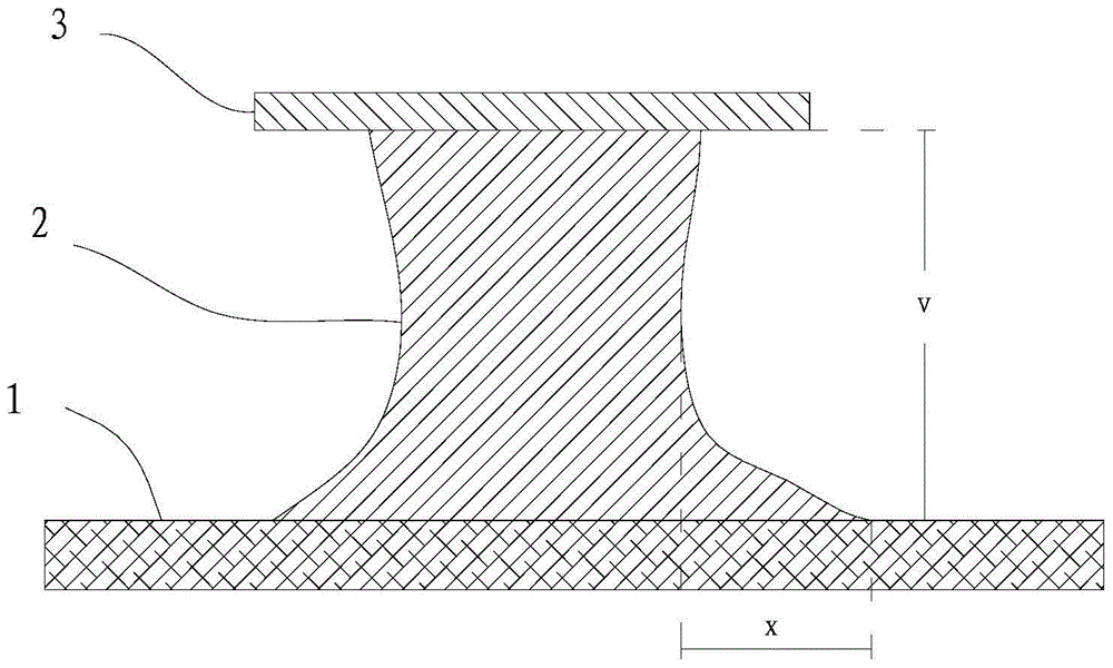
Figure 1 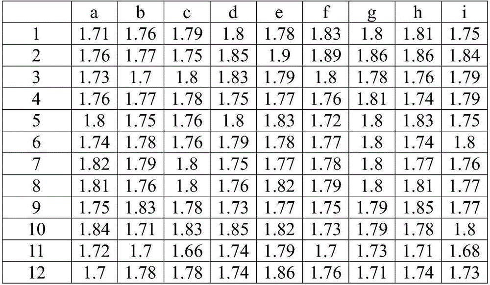
Figure 2 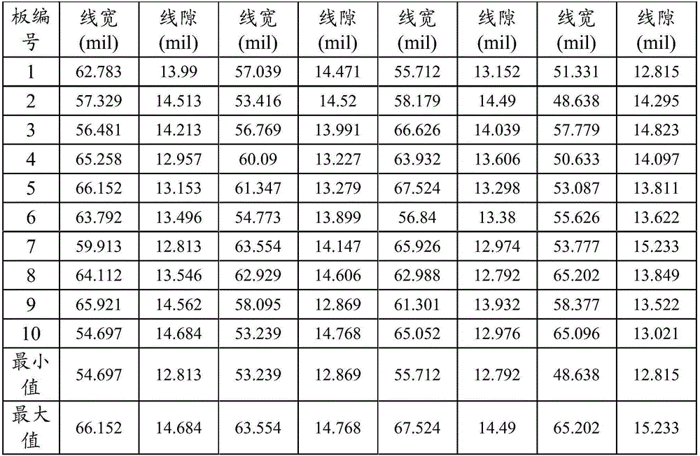
Figure 3
Abstract
Description
technical field
[0001] The invention relates to the technical field of PCB printed circuit boards, in particular to a thick copper circuit board with inconsistent inner and outer copper thicknesses and a preparation method thereof. Background technique
[0002] Automotive electronic components, especially in high-power and high-voltage parts such as engine power supply parts and automotive central electrical power supply parts, often use thick copper circuit boards with inconsistent inner and outer copper thicknesses (such as outer layer 6OZ, inner layer 12OZ thick copper circuit boards, etc.) ), the circuit is required to have high reliability characteristics such as heat aging resistance and low temperature cycle resistance.
[0003] In the conventional technology, the pressing process of the above-mentioned thick copper circuit board with inconsistent inner and outer layer copper thickness is to laminate the copper foil, prepreg and oxidized inner layer board in order and...
Examples
Embodiment 1
[0064] A method for preparing a thick copper circuit board (inner layer 12OZ, outer layer 6OZ thick copper board) with inconsistent copper thicknesses on the inner and outer layers, the circuit board adopts a four-layer structure, wherein the first and fourth circuit layers use 6OZ thick copper foil 12OZ thick copper foil is used for the second and third circuit layers, and the board thickness is 65-81mil.
[0065] The preparation method of this embodiment includes the steps of plate pressing, drilling and etching, and the other steps are prepared according to conventional methods. in:
[0066] (1) In the pressing process, the 1080 prepreg with a resin content of 68% is selected, and the hot pressing process and the cold pressing process are used for pressing in turn; the specific process parameters are shown in the table below.
[0067] Table 1. Setting of pressing plate process parameters
[0068]
[0069]
[0070] In the above-mentioned cold pressing process, the co...
Embodiment 2
[0077] A method for preparing a thick copper circuit board (inner layer 12OZ, outer layer 6OZ thick copper board) with inconsistent copper thicknesses on the inner and outer layers, the circuit board adopts a four-layer structure, wherein the first and fourth circuit layers use 6OZ thick copper foil 12OZ thick copper foil is used for the second and third circuit layers, and the board thickness is 65-81mil.
[0078] The preparation method of this embodiment includes the steps of plate pressing, drilling and etching, and the other steps are prepared according to conventional methods. in:
[0079] (1) In the pressing process, the 1080 prepreg with a resin content of 71% is selected, and the hot pressing process and the cold pressing process are used for pressing in turn; the specific process parameters are shown in the table below.
[0080] Table 3. Setting of pressing plate process parameters
[0081]
[0082] (2) In the drilling process, the board is baked at 120°C for 6 h...
Embodiment 3
[0088] A method for preparing a thick copper circuit board (inner layer 12OZ, outer layer 6OZ thick copper board) with inconsistent copper thicknesses on the inner and outer layers, the circuit board adopts a four-layer structure, wherein the first and fourth circuit layers use 6OZ thick copper foil 12OZ thick copper foil is used for the second and third circuit layers, and the board thickness is 65-81mil.
[0089] The preparation method of this embodiment includes the steps of plate pressing, drilling and etching, and the other steps are prepared according to conventional methods. in:
[0090] (1) In the pressing process, the 1080 prepreg with a resin content of 65% is selected, and the hot pressing process and the cold pressing process are used for pressing in turn; the specific process parameters are shown in the table below.
[0091] Table 5. Setting of pressing plate process parameters
[0092]
[0093] (2) In the drilling process, bake the board at 160°C for 4 hours...