
Shallow-trench half-super-junction VDMOS device and manufacturing method thereof
A manufacturing method and semi-superjunction technology, applied in semiconductor/solid-state device manufacturing, semiconductor devices, electrical components, etc., can solve the problems of weak current conduction per unit area and large forward conduction resistance.
Patent Information
- Authority / Receiving Office
- CN · China
- Current Assignee / Owner
- Publication Date
- 2016-05-11
- Estimated Expiration
- Not applicable · inactive patent
Smart Images
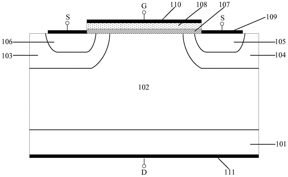
Figure 1 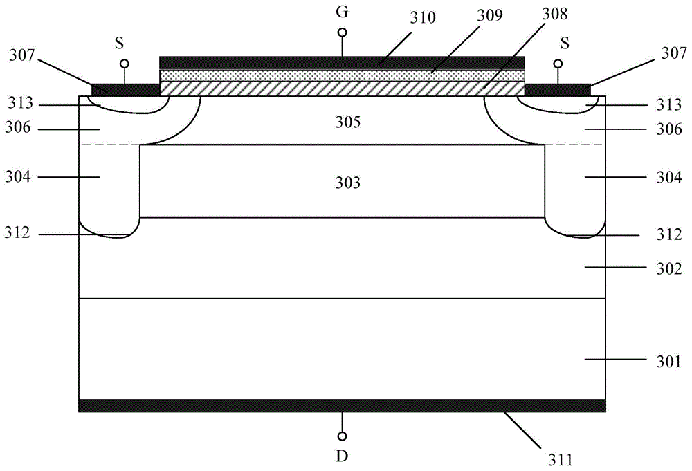
Figure 2 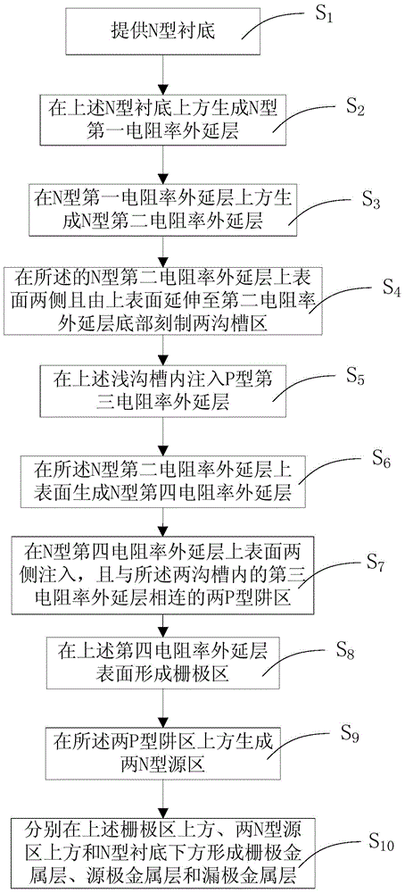
Figure 3
Abstract
Description
technical field
[0001] The invention relates to the technical field of semiconductor devices and manufacturing techniques thereof, in particular to a shallow trench semi-superjunction VDMOS device and a manufacturing method thereof. Background technique
[0002] VDMOS (VerticalDouble-diffused MetalOxideSemiconductor, vertical double-diffused metal oxide semiconductor) device is a power semiconductor device that has the advantages of both bipolar transistors and ordinary MOS devices. Compared with bipolar transistors, it has fast switching speed, small switching loss, high input impedance, low driving power, good frequency characteristics, high transconductance linearity, no secondary breakdown problem of bipolar power devices, and safe The work area is large. Therefore, VDMOS devices are ideal power semiconductor devices for both switching and linear applications.
[0003] For VDMOS devices, one of its important indicators is the on-resistance. With the development of VDM...
Examples
Embodiment Construction
[0041] In order to make the above objects, features and advantages of the present invention more comprehensible, specific implementations of the present invention will be described in detail below in conjunction with the accompanying drawings.
[0042] In the following description, many specific details are set forth in order to fully understand the present invention, but the present invention can also be implemented in other ways that are different from those described here, and those skilled in the art can do so without departing from the connotation of the present invention. By analogy, the present invention is not limited by the specific examples disclosed below.
[0043] As mentioned in the background section, the on-resistance of traditional VDMOS is limited by the silicon limit with the growth of withstand voltage, that is, the on-resistance increases rapidly with the increase of withstand voltage, and in order to prevent the resistance region from being broken down, the...