
Conical micro-pore array and preparation method thereof
A microhole array, tapered technology, applied in the field of material processing
Patent Information
- Authority / Receiving Office
- CN · China
- Patent Type
- Applications(China)
- Current Assignee / Owner
- Publication Date
- 2016-10-12
Smart Images
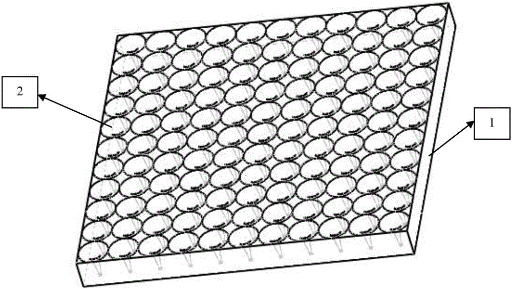
Figure 1 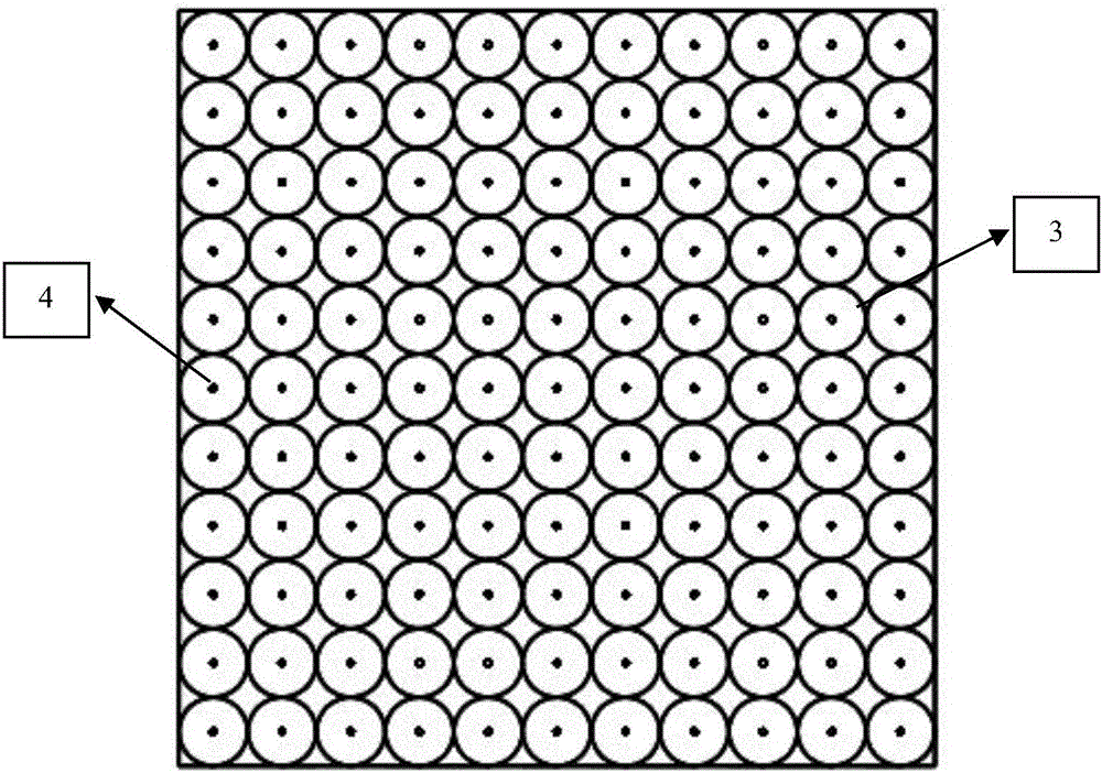
Figure 2 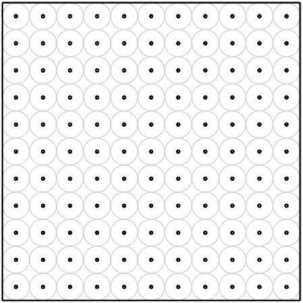
Figure 3
Abstract
Description
technical field
[0001] The invention belongs to the technical field of material processing, and relates to a tapered microhole array and a preparation method thereof. technical background
[0002] With the continuous progress and improvement of non-metallic thin film preparation methods, the continuous improvement of film quality has created conditions for the wide application of non-metallic thin films, and the different requirements for the application of non-metallic thin films in different fields are also promoting the continuous improvement of thin film preparation technology. Develop and mature. The advantages of non-metallic films include high hardness, very good physical and chemical properties, such as low coefficient of friction and high thermal conductivity. According to this characteristic, some high-hardness film materials are widely used.
[0003] On the other hand, non-metallic films also have very good biocompatibility. For example, some non-metallic films...
Examples
Embodiment
[0030] The diamond film is selected as a non-metallic film with a size of 5x5mm and a thickness of 0.2mm; before the non-metallic film is processed, the upper and lower surfaces of the film are ground and polished to make the surface roughness 0.1-1μm, and then soaked in alcohol and ultrasonically cleaned for 20 minutes to remove the attached Impurities and oil stains are then dried to obtain a non-metallic film for use;
[0031] Create a graphic file of the microwell array, use the graphic design software to design the microwell entrance pattern with an aperture diameter of 20 μm, and a distance between the centerlines of the microholes of 100 μm, turn on the fiber pulse laser (Hantong HT-20F laser equipment), and place the non-metallic film on the working surface. On the stage, adjust the focus of the laser so that the laser focus falls on the surface of the film, import the graphics file, set the wavelength of the fiber pulse laser to 1064nm, the power to 20w, and set the la...