
MOS transistor and its formation method
A MOS transistor and semiconductor technology, which is applied in the direction of semiconductor devices, semiconductor/solid-state device manufacturing, electrical components, etc., can solve the problems of poor performance and reliability of MOS transistors, achieve the effects of reducing junction capacitance, simplifying control, and increasing the depth of injection
Patent Information
- Authority / Receiving Office
- CN · China
- Patent Type
- Patents(China)
- Current Assignee / Owner
- Publication Date
- 2019-08-27
Smart Images
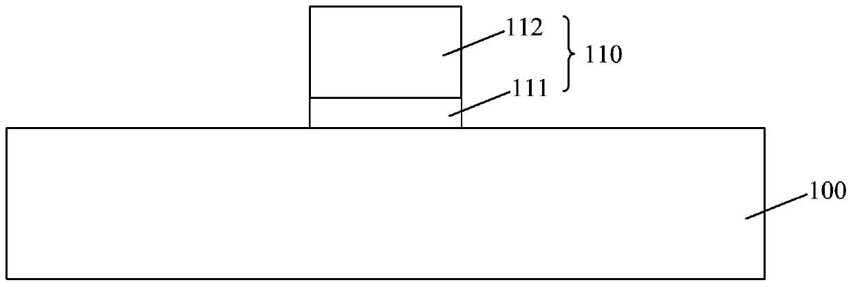
Figure 1 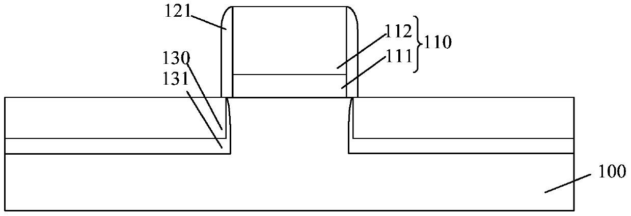
Figure 2 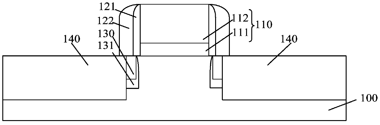
Figure 3
Abstract
Description
technical field
[0001] The invention relates to the field of semiconductor manufacturing, in particular to a MOS transistor and a forming method thereof. Background technique
[0002] MOS (Metal-Oxide-Semiconductor) transistor is one of the most important elements in modern integrated circuits. The basic structure of MOS transistors includes: a semiconductor substrate; a gate structure located on the surface of the semiconductor substrate, and the gate structure includes : the gate dielectric layer on the surface of the semiconductor substrate and the gate electrode layer on the surface of the gate dielectric layer; the lightly doped region on the semiconductor substrate on both sides of the gate structure and the source and drain on the semiconductor substrate on both sides of the gate structure Area.
[0003] The method for forming the MOS transistor is: providing a semiconductor substrate, forming a gate structure on the surface of the semiconductor substrate, the gate s...
Examples
Embodiment Construction
[0035] The performance and reliability of the MOS transistors formed in the prior art are poor as the feature size is further reduced.
[0036] Figure 1 to Figure 4 It is a schematic cross-sectional structure diagram of the formation process of a MOS transistor according to an embodiment of the present invention.
[0037] refer to figure 1 , providing a semiconductor substrate 100, forming a gate structure 110 on the surface of the semiconductor substrate 100, the gate structure 110 including a gate dielectric layer 111 on the surface of the semiconductor substrate 100 and a gate electrode layer 112 on the surface of the gate dielectric layer 111 .
[0038] refer to figure 2, forming offset spacers 121 on the sidewall surface of the gate structure 110, using the offset spacers 121 and the gate structure 110 as a mask, lightly doping the semiconductor substrate 100 on both sides of the gate structure 110 Lightly Doped Drain (LDD) implantation forms a lightly doped region ...