
Preparation method of a three-dimensional gate-all-around semiconductor field-effect transistor
A field-effect transistor and semiconductor technology, which is used in the manufacture of semiconductor/solid-state devices, semiconductor devices, electrical components, etc., to achieve the effects of high designability, improved performance, and reduced electric field diffusion
Patent Information
- Authority / Receiving Office
- CN · China
- Patent Type
- Patents(China)
- Current Assignee / Owner
- Publication Date
- 2020-06-19
Smart Images
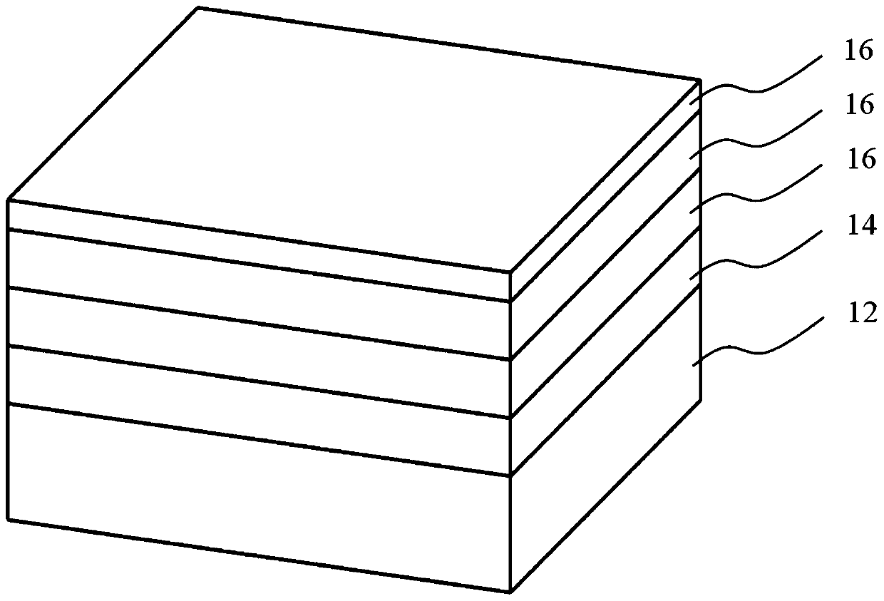
Figure 1 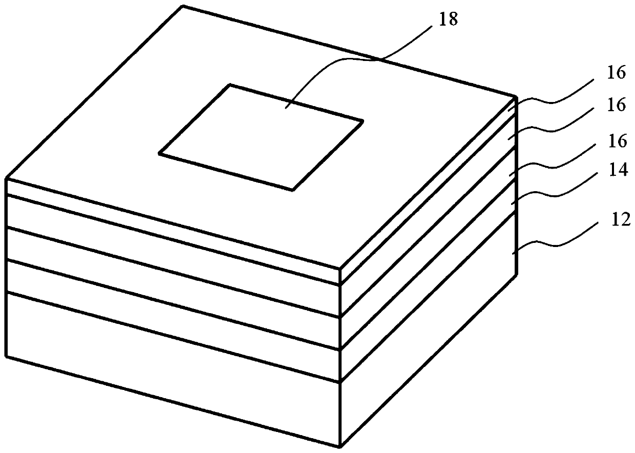
Figure 2 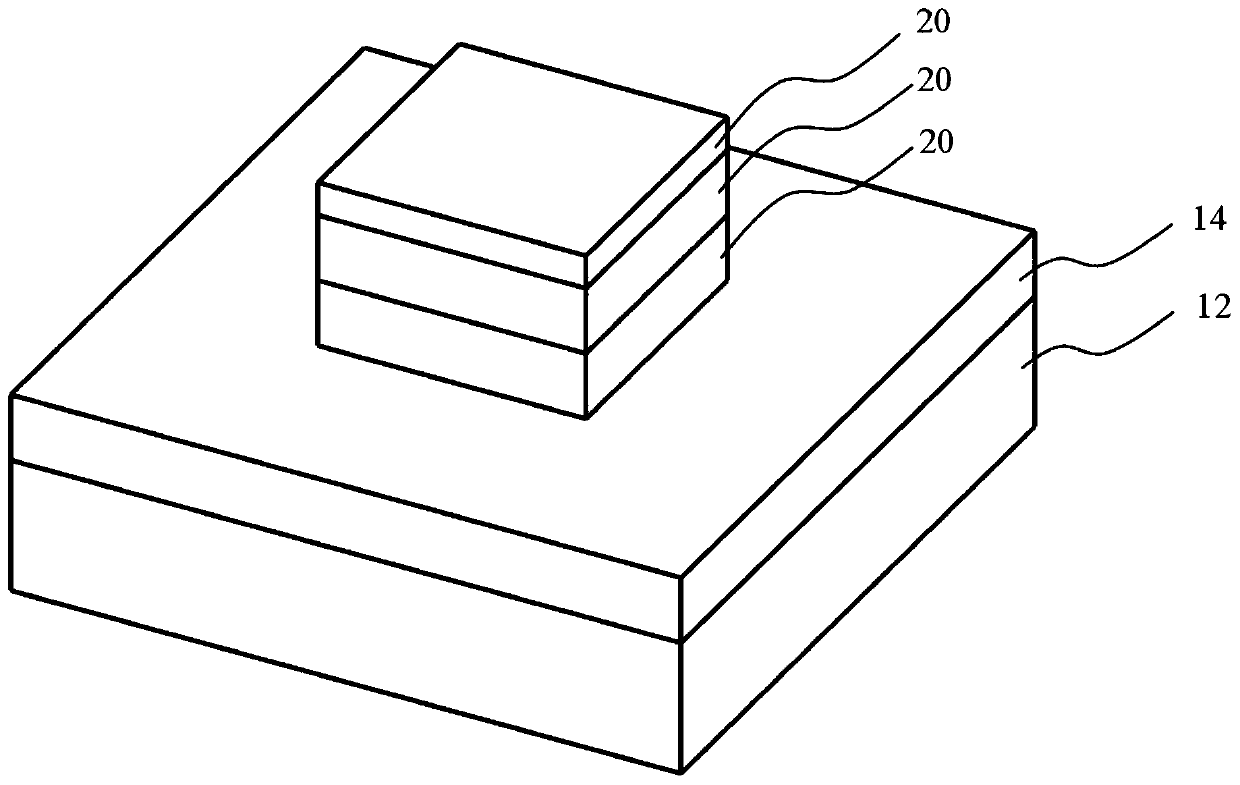
Figure 3
Abstract
Description
technical field
[0001] The invention relates to the technical field of three-dimensional micro-nano devices, in particular to a preparation method of a three-dimensional gate-around semiconductor field effect transistor. Background technique
[0002] At present, semiconductor integration technology is still full of challenges, and the demand for high integration and high performance is gradually increasing. As we all know, as the size of semiconductor devices continues to shrink, the method of improving device performance by scaling down the device size is approaching the limit, and the short-channel effect and subthreshold performance degradation also limit the further reduction of the device size. Therefore, more and more researchers use transistors with complex geometrical gate structures and ingenious processes to achieve high integration and high performance of devices. Among all the multi-gate structures proposed so far, the ring-shaped gate has the advantages of high...
Examples
Embodiment Construction
[0041] Figure 10 A schematic structural diagram of a three-dimensional gate-all-around semiconductor field effect transistor according to an embodiment of the present invention is shown. The preparation process specifically includes the preparation steps of the electrical insulation layer 14 and the functional structure layer 16 . figure 1 is a schematic diagram of preparing an electrical insulating layer 14 and a functional structural layer 16 on a substrate 12 according to an embodiment of the present invention. refer to figure 1, a silicon substrate can be selected as the supporting base 12 for the growth of the electrical insulating layer 14 and the functional structure layer 16 . The electrical insulating layer 14 can be selected from electrical insulating materials, such as silicon dioxide, undoped diamond, and the like. On the surface of the electrical insulation layer 14, one or more layers of functional structure layers 16 with different doping levels are grown. ...