
A semiconductor device and its manufacturing method and electronic device
A manufacturing method and semiconductor technology, applied in semiconductor/solid-state device manufacturing, semiconductor devices, electric solid-state devices, etc., can solve problems such as poor device mismatch performance and large work function fluctuations
Patent Information
- Authority / Receiving Office
- CN · China
- Patent Type
- Patents(China)
- Current Assignee / Owner
- Publication Date
- 2021-02-02
Smart Images
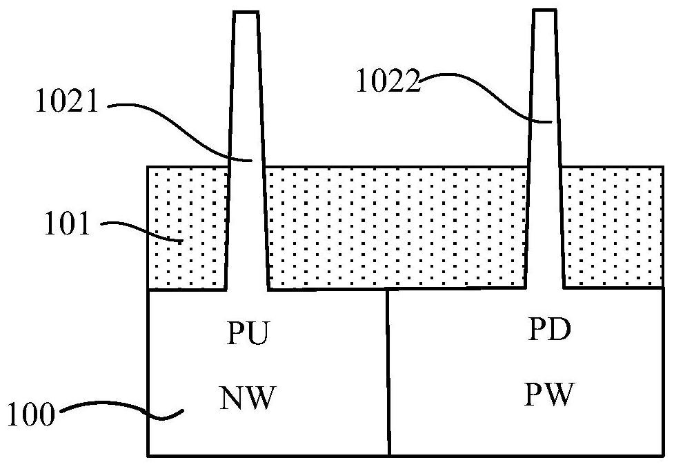
Figure 1 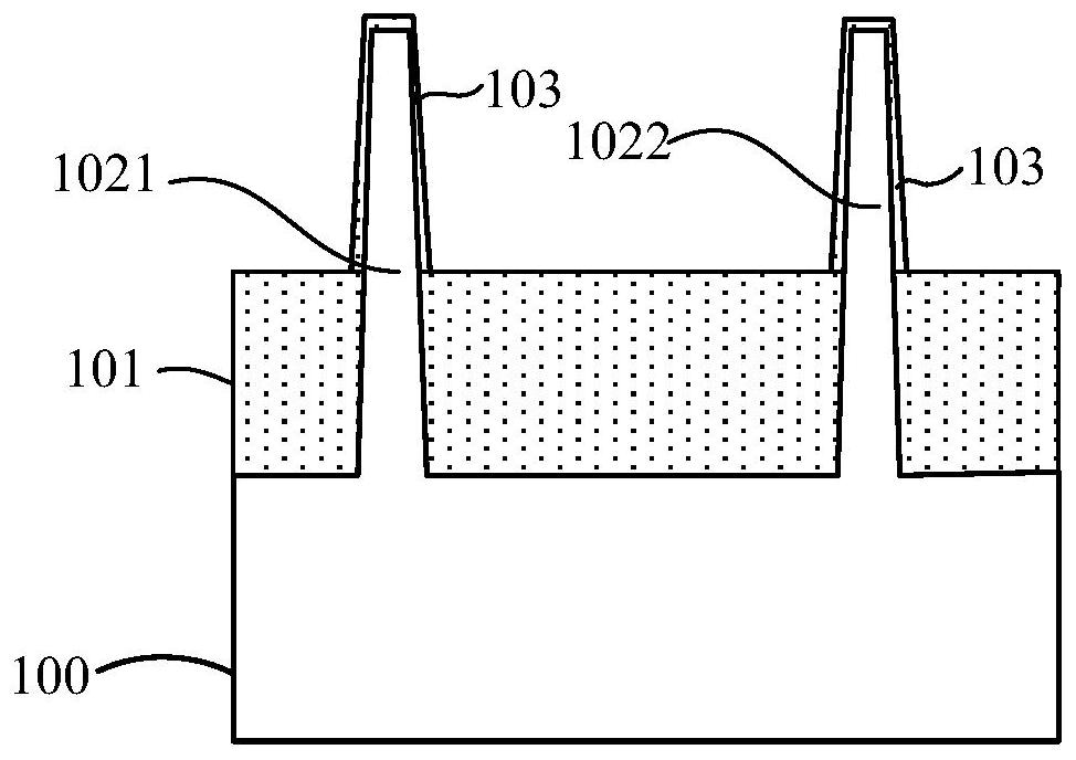
Figure 2 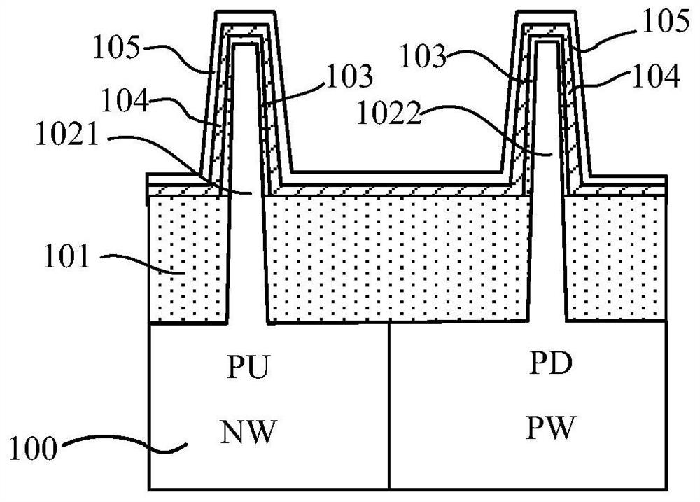
Figure 3
Abstract
Description
technical field
[0001] The present invention relates to the technical field of semiconductors, in particular to a semiconductor device, a manufacturing method thereof, and an electronic device. Background technique
[0002] In the field of semiconductor technology, static random access memory (SRAM) devices, as a typical semiconductor device, are widely used in electronic devices such as computers, mobile phones, and digital cameras. Currently, there are some designs that use fin field effect transistors (FinFETs) as transistor devices of SRAM cells to improve the density and performance of SRAMs.
[0003] In FinFET devices, the work function layer is very important for the adjustment of the device. In the process of device preparation, the post-metal gate process is usually used to form the work function layer. In order to meet the different requirements of PMOS devices and NMOS devices for the work function layer, it is often necessary to use For example, in the preparati...
Examples
Embodiment 1
[0067] Below, refer to Figure 1A-Figure 1J The manufacturing method of the semiconductor device of the present invention is described in detail, wherein, Figure 1A-Figure 1J A cross-sectional view showing a structure formed in relevant steps of a method for manufacturing a semiconductor device in an embodiment of the present invention; figure 2 A top view of a structure obtained by a method for manufacturing a semiconductor device in an embodiment of the present invention is shown.
[0068] Specifically, first, as Figure 1A As shown, a semiconductor substrate 100 is provided, the semiconductor substrate 100 includes a PMOS region and an NMOS region, and a first fin structure 1021 is respectively formed in the PMOS region and the NMOS region on the semiconductor substrate 100 and the second fin structure 1022 .
[0069] In this example, the method of the present invention is described in detail by taking the manufacture of SRAM devices as an example, wherein, the PMOS regi...
Embodiment 2
[0136] The present invention also provides a semiconductor device formed by using the method in the first implementation, and the semiconductor device may be an SRAM device.
[0137] Below, refer to as Figure 1J and figure 2 The semiconductor device of the present invention will be described in detail.
[0138] First, the semiconductor device of the present invention includes: a semiconductor substrate 100, the semiconductor substrate 100 includes a PMOS region and an NMOS region, and first fins are respectively formed in the PMOS region and the NMOS region on the semiconductor substrate structure 1021 and a second fin structure 1022 .
[0139] When the semiconductor device is an SRAM device, the PMOS area refers to the pull-up transistor (PU) area of the SRAM device, and the NMOS area refers to the down transistor (PD) area of the SRAM device.
[0140] Further, various well regions are formed in the semiconductor substrate, for example, an N-type well region (NW) is ...
Embodiment 3
[0174] The present invention also provides an electronic device, including the semiconductor device described in Embodiment 2, and the semiconductor device is prepared according to the method described in Embodiment 1.
[0175] The electronic device of this embodiment can be any electronic device such as a mobile phone, a tablet computer, a notebook computer, a netbook, a game console, a TV set, a VCD, a DVD, a navigator, a digital photo frame, a camera, a video camera, a recording pen, MP3, MP4, PSP, etc. Product or equipment, but also any intermediate product including electrical circuits. The electronic device according to the embodiment of the present invention has better performance due to the use of the above-mentioned semiconductor device.
[0176] in, Figure 4 An example of a mobile phone handset is shown. The mobile phone handset 400 is provided with a display portion 402 included in a housing 401, operation buttons 403, an external connection port 404, a speaker 4...