
Thin film transistor and preparation method thereof
A technology of thin film transistors and amorphous silicon layers, which is applied in the direction of transistors, semiconductor/solid-state device manufacturing, semiconductor devices, etc., and can solve problems such as instability of hydrogenated amorphous silicon layers
Patent Information
- Authority / Receiving Office
- CN · China
- Current Assignee / Owner
- Publication Date
- 2018-12-28
Smart Images
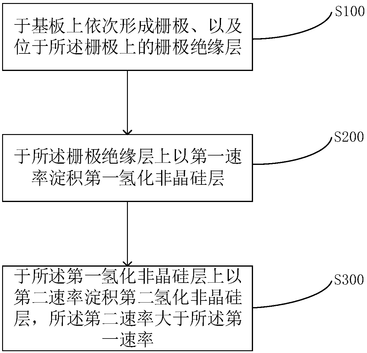
Figure 1 
Figure 2 
Figure 3
Abstract
Description
Technical field
[0001] The invention relates to the field of display, in particular to a thin film transistor and a preparation method thereof. Background technique
[0002] With the development of technology in recent years, thin-film transistor displays have gradually occupied a leading position in the display field because of their low power consumption and excellent display quality. Generally, thin film transistor displays use amorphous silicon thin film transistors as switches. Amorphous silicon thin film transistors usually have the performance of large area uniformity, large capacity, and high display quality, and are the key devices of large-size active liquid crystal display devices.
[0003] However, the hydrogenated amorphous silicon layer in the amorphous silicon thin film transistor is unstable, it will absorb more energy when exposed to light, and generate more electron-hole pairs than when it is not illuminated, which will cause the threshold voltage to shift and ca...
Examples
Embodiment Construction
[0038] In order to make the above-mentioned objects, features and advantages of the present invention more obvious and understandable, the specific embodiments of the present invention will be described in detail below with reference to the accompanying drawings. In the following description, many specific details are explained in order to fully understand the present invention. However, the present invention can be implemented in many other ways different from those described herein, and those skilled in the art can make similar improvements without departing from the connotation of the present invention. Therefore, the present invention is not limited by the specific embodiments disclosed below.
[0039] It should be noted that when an element is referred to as being "disposed on" another element, it may be directly on the other element or a central element may also exist. When an element is considered to be "connected" to another element, it can be directly connected to the ot...