
SOI active adapter plate for three-dimensional packaging and preparation method thereof
A three-dimensional packaging and transition board technology, which is applied in semiconductor/solid-state device manufacturing, electrical components, and electrical solid-state devices, etc., can solve problems such as short-channel effect latch-up effect, affect device performance, etc., to suppress short-channel effect. and the effect of latch-up
Patent Information
- Authority / Receiving Office
- CN · China
- Patent Type
- Applications(China)
- Current Assignee / Owner
- Publication Date
- 2020-11-03
Smart Images
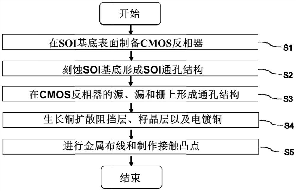
Figure 1 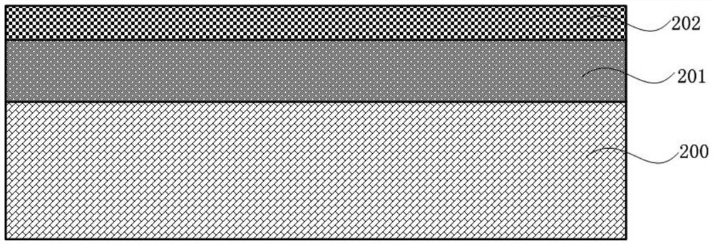
Figure 2 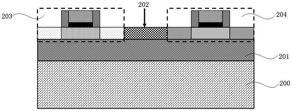
Figure 3
Abstract
Description
technical field
[0001] The invention belongs to the field of integrated circuit packaging, and in particular relates to an SOI active adapter board for three-dimensional packaging and a preparation method thereof. Background technique
[0002] With the rapid development of integrated circuit technology, microelectronic packaging technology has gradually become the main factor restricting the development of semiconductor technology. In order to realize the high density of electronic packaging, obtain better performance and lower overall cost, technicians have developed a series of advanced packaging technologies. Among them, the three-dimensional system-in-package technology has good electrical performance and high reliability, and can achieve high packaging density at the same time, and is widely used in various high-speed circuits and miniaturized systems.
[0003] Through Silicon Via (TSV) interposer technology is a new technology for interconnection of stacked chips in t...
Examples
Embodiment Construction
[0015] In order to make the purpose, technical solutions and advantages of the present invention clearer, the technical solutions in the embodiments of the present invention will be clearly and completely described below in conjunction with the accompanying drawings in the embodiments of the present invention. It should be understood that the specific The examples are only used to explain the present invention, not to limit the present invention. The described embodiments are only some, not all, embodiments of the present invention. Based on the embodiments of the present invention, all other embodiments obtained by persons of ordinary skill in the art without making creative efforts belong to the protection scope of the present invention.
[0016] In the description of the present invention, it should be noted that the orientation or positional relationship indicated by the terms "upper", "lower", "vertical" and "horizontal" are based on the orientation or positional relation...