
Local large-area welding plate-level interconnection integration method for airtight packaging unit
A technology of hermetic packaging and integration method, applied in electrical components, semiconductor/solid-state device manufacturing, circuits, etc., can solve the problem of low reliability of signal interconnection, improve the tensile and shear strength of pads, and improve reliability Sexuality, reduced peeling or tearing effect
Patent Information
- Authority / Receiving Office
- CN · China
- Current Assignee / Owner
- Publication Date
- 2020-11-13
Smart Images
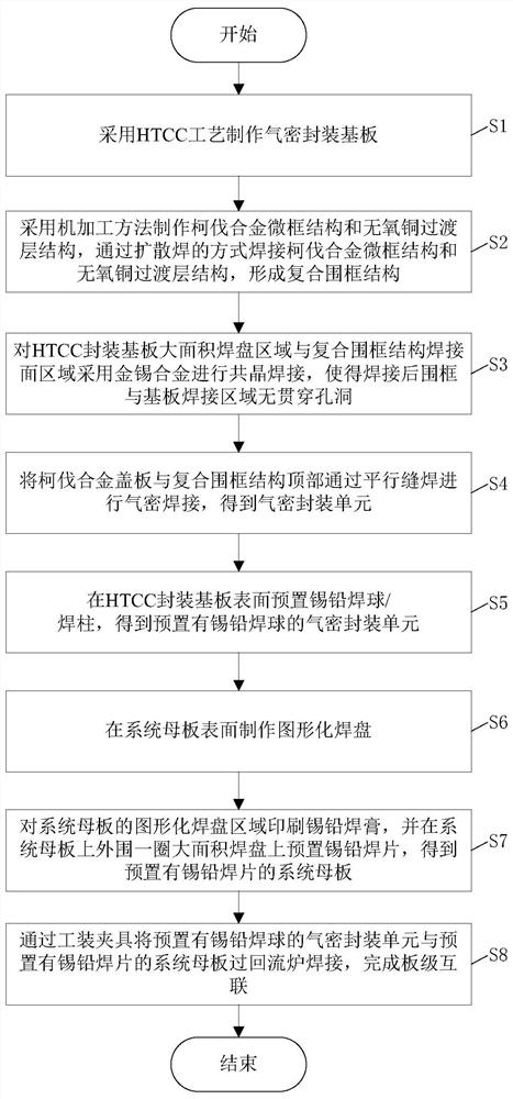
Figure 1 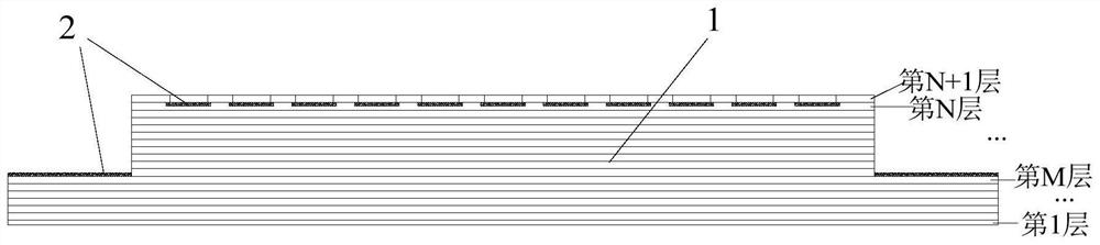
Figure 2 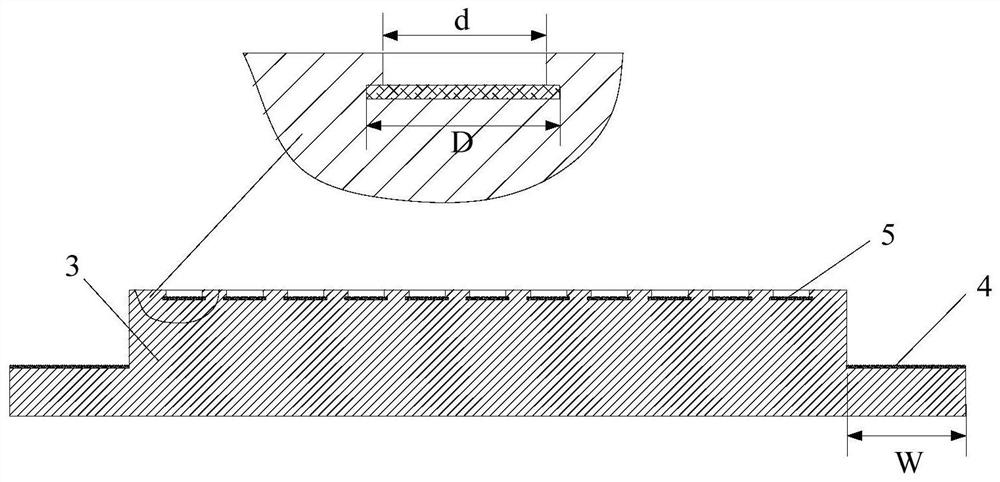
Figure 3
Abstract
Description
technical field
[0001] The invention relates to the technical field of board-level interconnection of electronic packaging, in particular to an integrated method for local large-area welding board-level interconnection of hermetic packaging units. Background technique
[0002] Electronic complete machines put forward higher requirements for packaging miniaturization, high density, multi-functionality, high reliability, and high power. The system-level packaging form using co-fired multilayer ceramic substrates has been widely favored. The signal interconnection between the multilayer ceramic package and the system motherboard is usually implemented by a ball grid array (BGA) interconnection. However, the thermal expansion coefficients of multilayer ceramic substrates and system motherboards differ greatly. As the complexity of package functions increases and the size of package substrates increases, when experiencing high and low temperature loads, the bonding pads and inter...
Examples
Embodiment Construction
[0046] The specific embodiments of the present invention are described below so that those skilled in the art can understand the present invention, but it should be clear that the present invention is not limited to the scope of the specific embodiments. For those of ordinary skill in the art, as long as various changes Within the spirit and scope of the present invention defined and determined by the appended claims, these changes are obvious, and all inventions and creations using the concept of the present invention are included in the protection list.
[0047] Such as figure 1 As shown, a local large-area soldered board-level interconnection integration method of a hermetic packaging unit includes the following steps:
[0048] In this embodiment, tin-lead solder balls are selected as interconnection solder joints.
[0049] S1, using HTCC technology to make hermetic package substrate; Figure 2 ~ Figure 4 As shown, the HTCC hermetic packaging substrate 3 is produced by th...