
Memory structure and manufacturing method thereof
A technology of memory and gate structure, applied in the field of semiconductor structure and its manufacturing, can solve the problem of spending a lot of energy and time
Patent Information
- Authority / Receiving Office
- CN · China
- Current Assignee / Owner
- Publication Date
- 2021-09-14
Smart Images
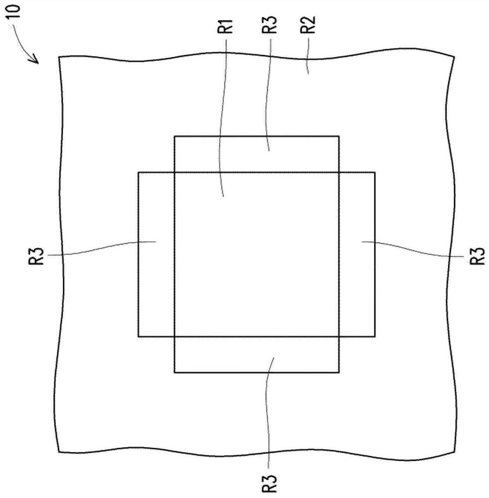
Figure 1 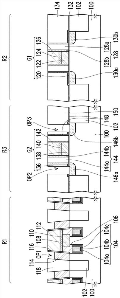
Figure 2 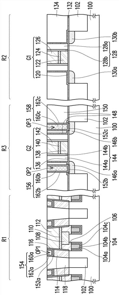
Figure 3
Abstract
Description
Technical field
[0001] The present invention relates to a semiconductor structure and a manufacturing method, and more particularly to a memory structure and a manufacturing method. Background technique
[0002] Current common data processing data processing is performed by a memory chip located on different processor. However, where a significant number of data processing, various data back and forth between memory and the processor takes a lot of energy and time.
[0003] Thus, to gradually develop a memory and a processor integrated in the same chip memory structures, such as a memory of a processor (processor in memory, PIM) memory or AI (artificial intelligencememory, AIM) a new chip architecture. However, to effectively integrate memory and a processor on the same chip, must be able to improve the effectiveness of the peripheral circuit transistor region. Inventive content
[0004] The present invention provides a memory structure and a manufacturing method which can impro...
Examples
Embodiment Construction
[0042] figure 1 A top view of a memory structure according to an embodiment of the present invention. Figures 2A to 2H Manufacturing process cross-sectional view of a memory structure according to an embodiment of the present invention. image 3 for Figure 2h A peripheral circuit region and the transistor structure of a transistor array region in a schematic view. exist image 3 Omitted Figure 2h The section member to clear image 3 The positional relationship between the components.
[0043] Please refer to figure 1 and Figure 2A , Substrate 100 is provided. Substrate 100 includes a memory cell region and the peripheral circuit region R1 R2. In addition, the substrate 100 may further include a transistor array region R3. R3 transistor array region R2 is located between the memory cell region and the peripheral circuit region R1. R3 may be located in the transistor array region around the memory cell region R1. R2 may be a peripheral circuit area other than the memory cell region R1...