
Planar display device with float-grid structure and its production
A flat-panel display and manufacturing process technology, applied in the manufacture of discharge tubes/lamps, image/graphic display tubes, ships or lead-in wires, etc., can solve problems such as scrapping, affecting device display image quality, and display device burnout. Achieve the effect of eliminating secondary electron emission, suppressing grid runaway phenomenon, and avoiding grid runaway phenomenon
Patent Information
- Authority / Receiving Office
- CN · China
- Current Assignee / Owner
- Publication Date
- 2007-01-17
- Estimated Expiration
- Not applicable · inactive patent
Smart Images
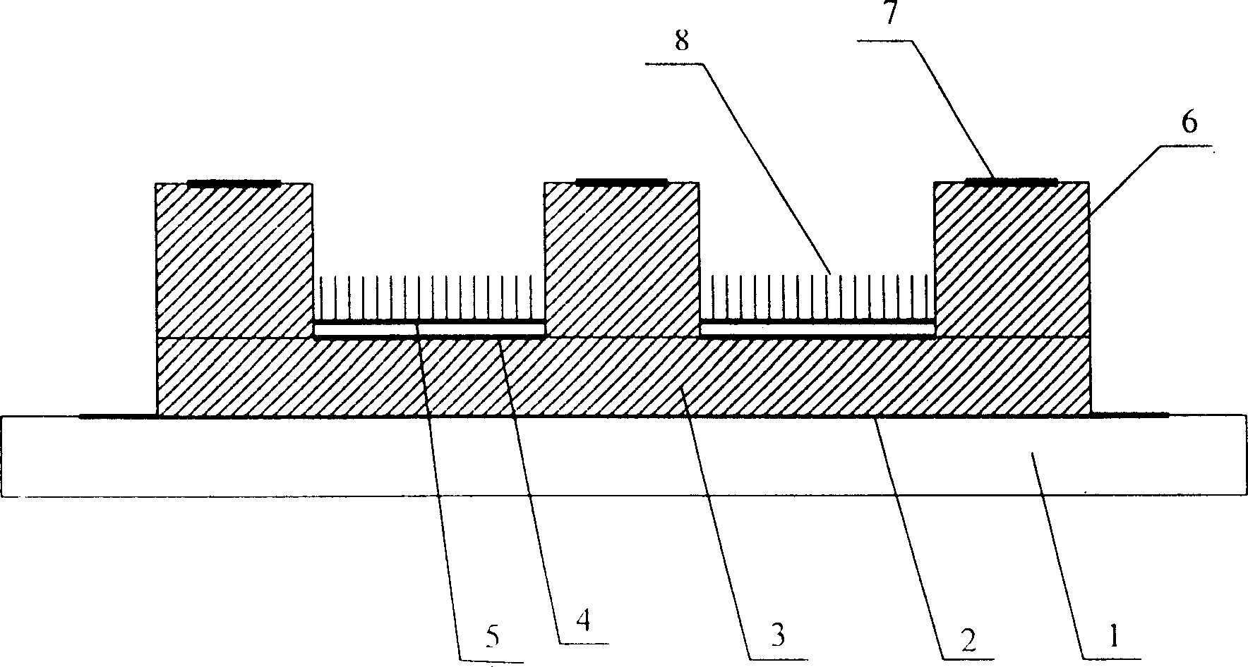
Figure 1 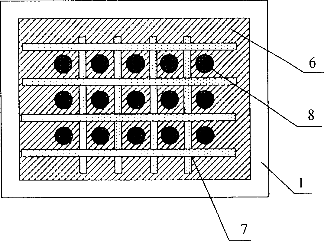
Figure 2 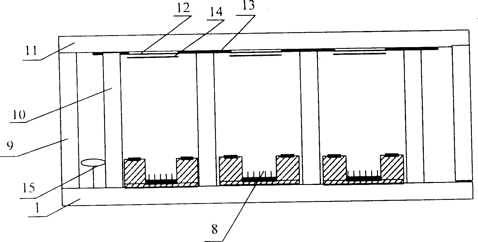
Figure 3
Abstract
Description
technical field
[0001] The invention belongs to the fields of plane display technology, microelectronic science and technology, vacuum science and technology, and nano science and technology, and relates to the manufacture of flat panel field emission displays, in particular to flat panels for carbon nanotube cathodes. The content of device fabrication of field emission display, especially related to the fabrication process of field emission flat panel display device with floating gate structure and carbon nanotube cathode. Background technique
[0002] Carbon nanotube is a coaxial tubular substance with unique geometric shape, small tip curvature radius, high aspect ratio and stable physical and chemical properties. It is an ideal material for emitting cathodes. At present, the preparation methods for carbon nanotube cathodes can be roughly divided into two categories, namely: direct growth method and transplantation method. The field emission characteristics of carbon nan...
Examples
Embodiment Construction
[0032] The present invention will be further described below in conjunction with the accompanying drawings and embodiments, but the present invention is not limited to these embodiments.
[0033] Such as figure 1 , 2 , 3, the present invention includes a sealed vacuum chamber made of a cathode panel 1, an anode panel 11 and a surrounding glass frame 9, an anode conductive layer 12 photoetched on the anode panel 11, and an anode conductive layer 12 prepared on the anode conductive layer 12. The phosphor layer 14, the supporting wall structure 10 between the cathode panel 1 and the anode panel 11, and the getter accessory element 15 are fixedly installed on the cathode panel to prevent secondary electron emission and grid out-of-control phenomenon. The structure is a floating gate structure controlled by the carbon nanotube cathode, and the floating gate structure is located above the carbon nanotube cathode.
[0034] The floating gate structure includes a gate conductive laye...