
Semiconductor structure
a semiconductor and structure technology, applied in the field of semiconductor structure, can solve the problems of deformation of the layer and its interface, deformation of the silicon photonic circuit, severe limitations on the thermal budget allowed for the integration and/or processing of devices, etc., to achieve the reduction of electrical and optical signals between the functional-oxide crystalline layer and the semiconductor substrate, and the flexibility and scope of application. , the effect of reducing the problem of decoupling electrical and optical signals
Patent Information
- Authority / Receiving Office
- US · United States
- Patent Type
- Patents(United States)
- Current Assignee / Owner
- Publication Date
- 2018-06-26
Smart Images
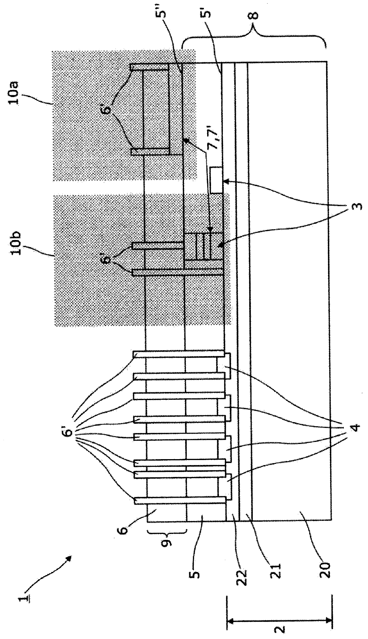
Figure 1 
Figure 2
Abstract
Description
CROSS-REFERENCE TO RELATED APPLICATION(S)
[0001] This application is a continuation of U.S. application Ser. No. 14 / 945,752 filed on Nov. 19, 2015, now U.S. Pat. No. 9,696,488, which claims benefit of priority of U.K. Patent Application Number GB 1420531.4, filed on Nov. 19, 2014, the disclosures of which are incorporated by reference herein.TECHNICAL FIELD
[0002] The present invention relates to a semiconductor structure and also extends to a method of fabricating such a structure.BACKGROUND
[0003] Silicon photonics is a baseline technology that may be applicable for addressing a bandwidth bottleneck occurring in relation to future electronic circuits and / or systems. Silicon photonic circuits are based on many different elementary devices that may be applied for manipulating light. In a usual scenario, many of these elementary devices operate based on a change in the refractive index of one of their constituent materials, by applying an electrical field or current thereto.
[0004] One of th...
Examples
Embodiment Construction
[0040]Within the description, the same reference numerals or signs have been used to denote the same parts or the like.
[0041]As can be seen from FIG. 1, a semiconductor structure 1 according to an embodiment of the present invention comprises a semiconductor substrate 2, which may be provided in a multi-layered configuration 20, 21, 22 of consecutively arranged layers of silicon 20, silicon dioxide 21 and a silicon substrate 22. The semiconductor substrate 2 is processed at a temperature of 700° C. to 1100° C. to comprise at least an optical aspect 3 comprising at least a silicon photonics device and at least an electronic aspect 4 comprising at least an electronic device 4. In the example shown in FIG. 1, the optical aspect 3 comprises multiple silicon photonic devices that are optical waveguides 3 and the electronic aspect 4 comprises multiple electronic transistors 4. On the processed semiconductor substrate 2, 3, 4, there is provided an interlayer dielectric layer 5—also known a...