
Semiconductor device
a technology of semiconductor devices and semiconductors, applied in semiconductor devices, electronic switching, pulse techniques, etc., can solve problems such as negative impact on radiation tolerance, and achieve the effect of maintaining radiation tolerance and reducing power consumption
Patent Information
- Authority / Receiving Office
- US · United States
- Patent Type
- Patents(United States)
- Current Assignee / Owner
- Publication Date
- 2020-11-10
Smart Images
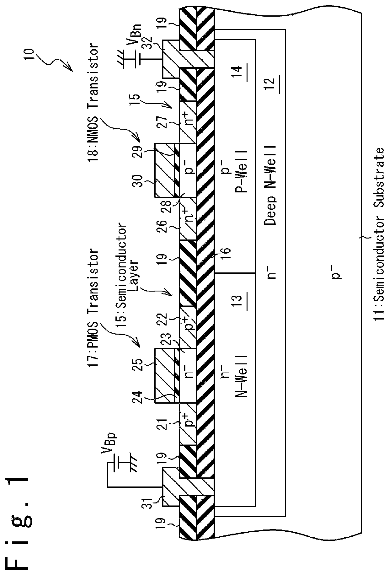
Figure 1 
Figure 2 
Figure 3
Abstract
Description
TECHNICAL FIELD
[0001] The present invention relates to a semiconductor device and an operation adjustment method thereof, more particularly, to control of a substrate bias voltage of a semiconductor device using a silicon-on-insulator (SOI) technology.BACKGROUND ART
[0002] The SOI technology is widely used as a technology for improving the operation speed of a semiconductor device and reducing the power consumption. In a semiconductor device using an SOI technology (which may be simply referred to as “SOI device”, hereinafter), a dielectric layer (buried dielectric layer) is formed under a channel of an MOS transistor, and this effectively reduces the parasitic capacitance of the MOS transistor. Accordingly, use of the SOI technology achieves rapid operation speed and reduced power consumption.
[0003] To further reduce power consumption, technologies to control substrate bias voltages of SOI devices have been studied. An approach to reduce power consumption through substrate bias voltage...
Examples
Embodiment Construction
lass="d_n">[0026]FIG. 1 is a section view illustrating the configuration of a semiconductor device 10, according to one embodiment of the present invention. The semiconductor device 10 according to this embodiment is configured as an SOI device. More specifically, a deep N-well 12 is formed in a semiconductor substrate 11, and an N-well 13 and a P-well 14 are formed in the deep N-well 12. In this embodiment, a p-type substrate is used as the semiconductor substrate 11. Alternatively, an n-type substrate may be used as the semiconductor substrate 11. The deep N-well 12 and the N-well 13 comprise n-type semiconductor regions doped with n-type impurities, and the P-well 14 comprises a p-type semiconductor region doped with p-type impurities. The N-well 13 and the P-well 14 are adjacent to each other and a pn junction is formed at the boundary between the N-well 13 and the P-well 14.
[0027]A semiconductor layer 15 is formed in the surface portion of the semiconductor substrate 11, and a ...