
Photoconductor on active pixel image sensor
a photoconductor and image sensor technology, applied in the field of photoconductor on active pixel image sensor, can solve the problems of large energy consumption of small cameras using ccd sensors, occupied circuitry, and inability to use photo-sensing
Patent Information
- Authority / Receiving Office
- US · United States
- Patent Type
- Applications(United States)
- Current Assignee / Owner
- Publication Date
- 2004-02-26
- Estimated Expiration
- Not applicable · inactive patent
Smart Images
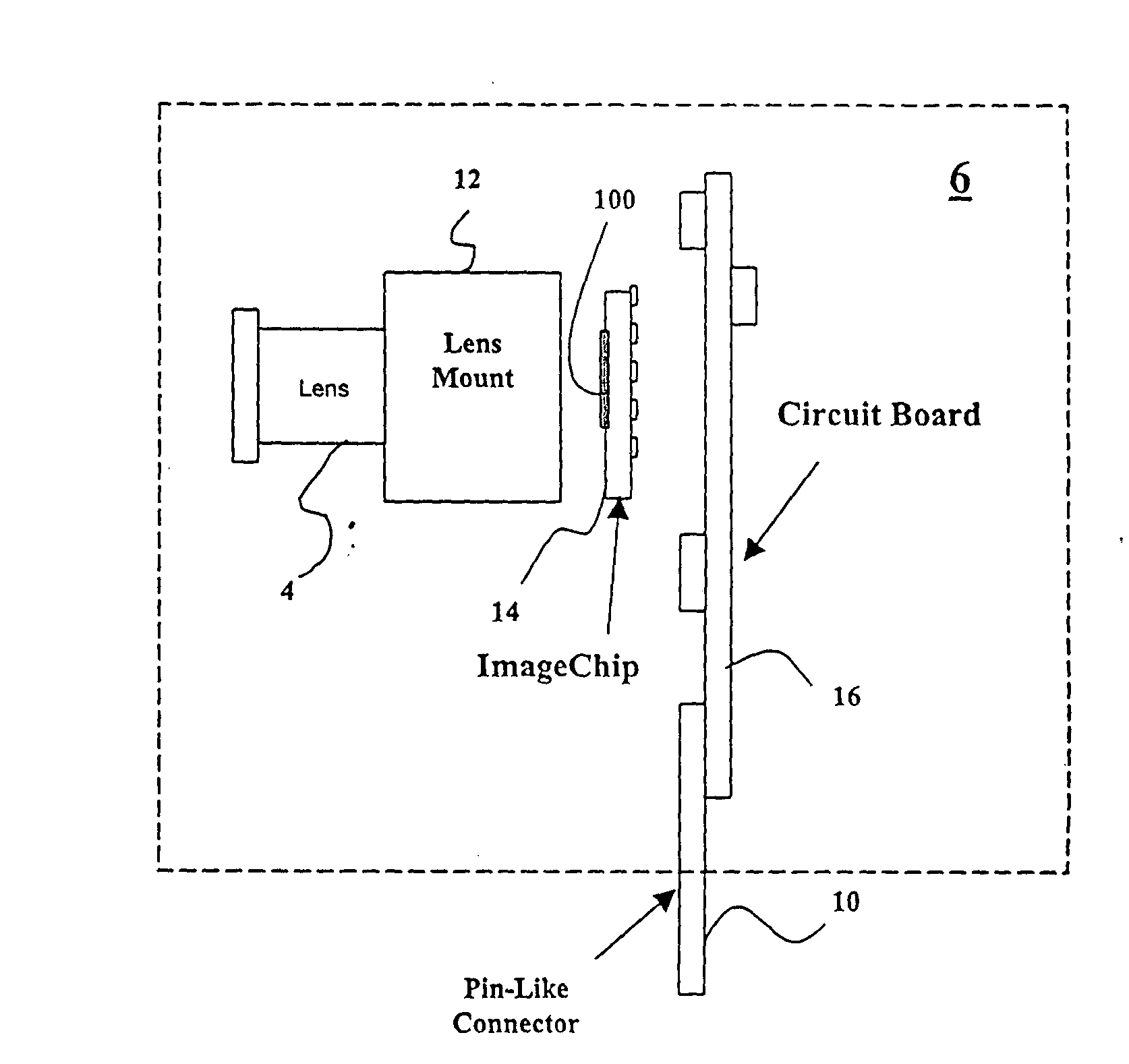
Figure 1 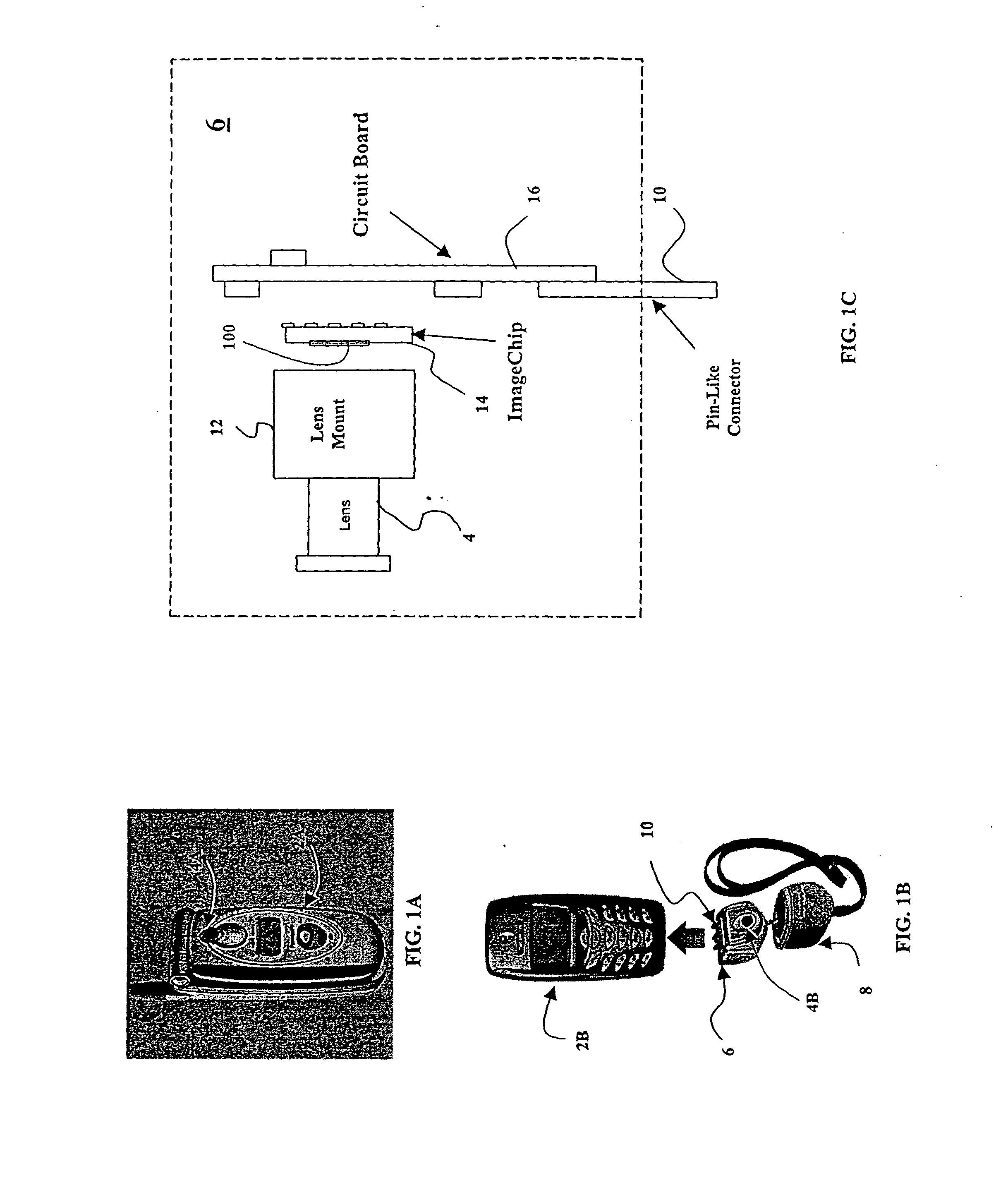
Figure 2 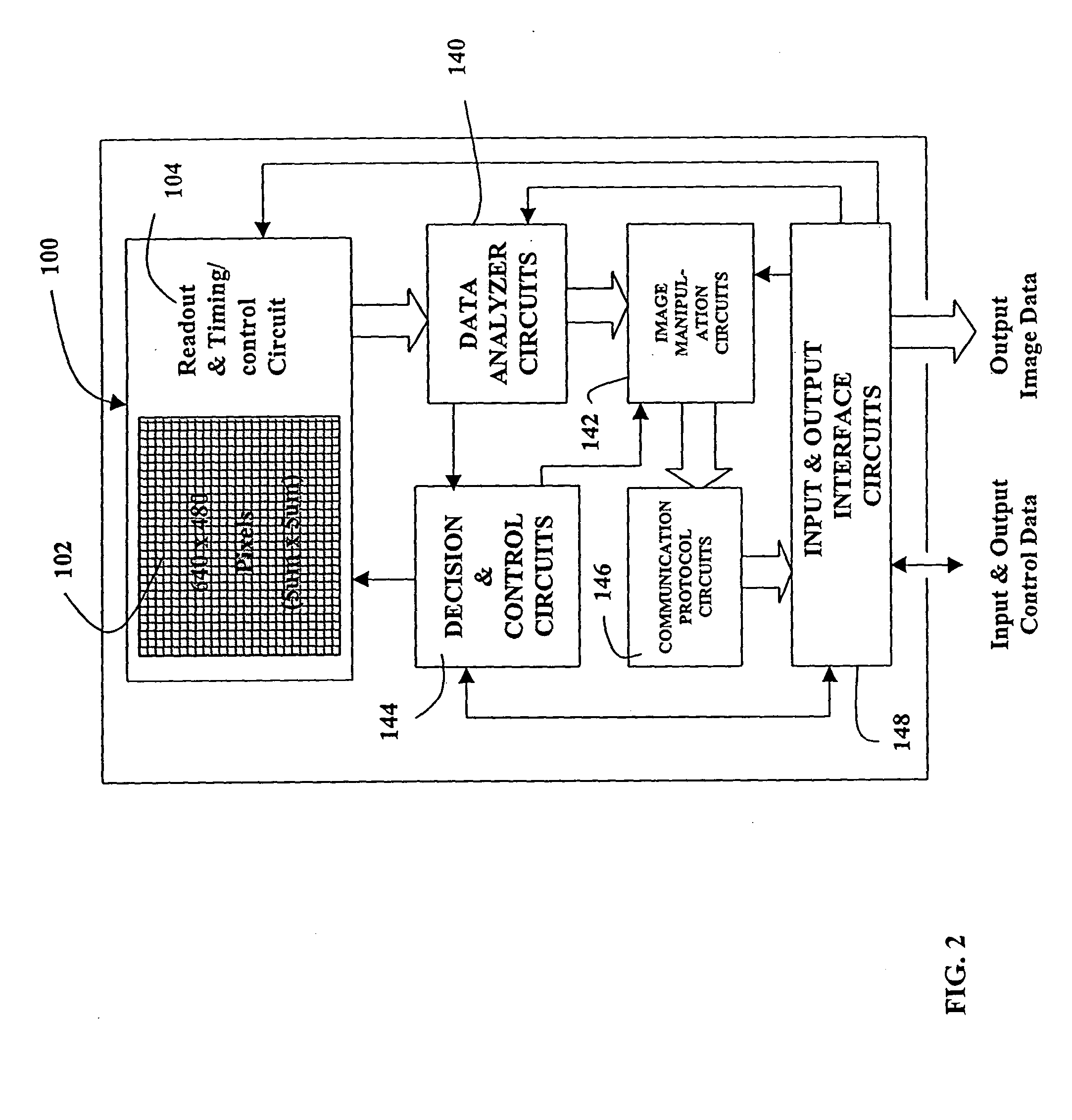
Figure 3
Abstract
Description
[0001] This application is a continuation in part of U.S. Pat. application Ser. No. 10 / 072,637 filed Feb. 5, 2002, Ser. No. 10 / 229,953 filed Aug. 27, 2002, Ser. No. 10 / 229,954 filed Aug. 27, 2002, Ser. No. 10 / 229,955 filed Aug. 27, 2002, Ser. No. 10 / 229,956 filed Aug. 27, 2002 and Ser. No. 10 / 371,618, filed Feb. 22, 2003. The present invention relates to image sensors and in particular to MOS and CMOS based image sensors.BACKGROUND OF THE INVENTION
[0002] A typical electronic image sensor is comprised of an array of a large number of very small light detectors, together called a "pixel array". These sensors typically generate electronic signals representative of each pixel that have amplitudes that are proportional to the intensity of the light received by each of the detectors in the array. In electronic cameras imaging components produce an optical image of a scene onto the pixel array. The electronic image sensor converts the optical image into a set of electronic signals. These e...
Examples
Embodiment Construction
[0048] Single Chip Camera with Photo Conductor on Active Pixel Sensor A preferred embodiment of the present invention is a single chip camera with a sensor consisting of a photodiode array consisting of photoconductive layers on top of an active array of CMOS circuits. (Applicants refer to this sensor as a "POAP Sensor" the "POAP" referring to "Photoconductor On Active Pixel".) In this particular POAP sensor there are 307,200 pixels arranged in as a 640.times.480 pixel array and there is a transparent electrode on top of the photoconductive layers. The pixels are 5 microns.times.5 microns and the packing fraction is approximately 100 percent. The active dimensions of the sensor are 3.2 mm.times.2.4 mm and a preferred lens unit is a standard lens with a {fraction (1 / 4.5)} inch optical format. A preferred application of the camera is as a component of a cellular phone as shown in FIGS. 1A and 1B. In the 1A drawing the camera is an integral part of the phone 2A and the lens is shown at...