
Electronic component testing apparatus
Patent Information
- Authority / Receiving Office
- US · United States
- Current Assignee / Owner
- Publication Date
- 2007-01-25
- Estimated Expiration
- Not applicable · inactive patent
Smart Images
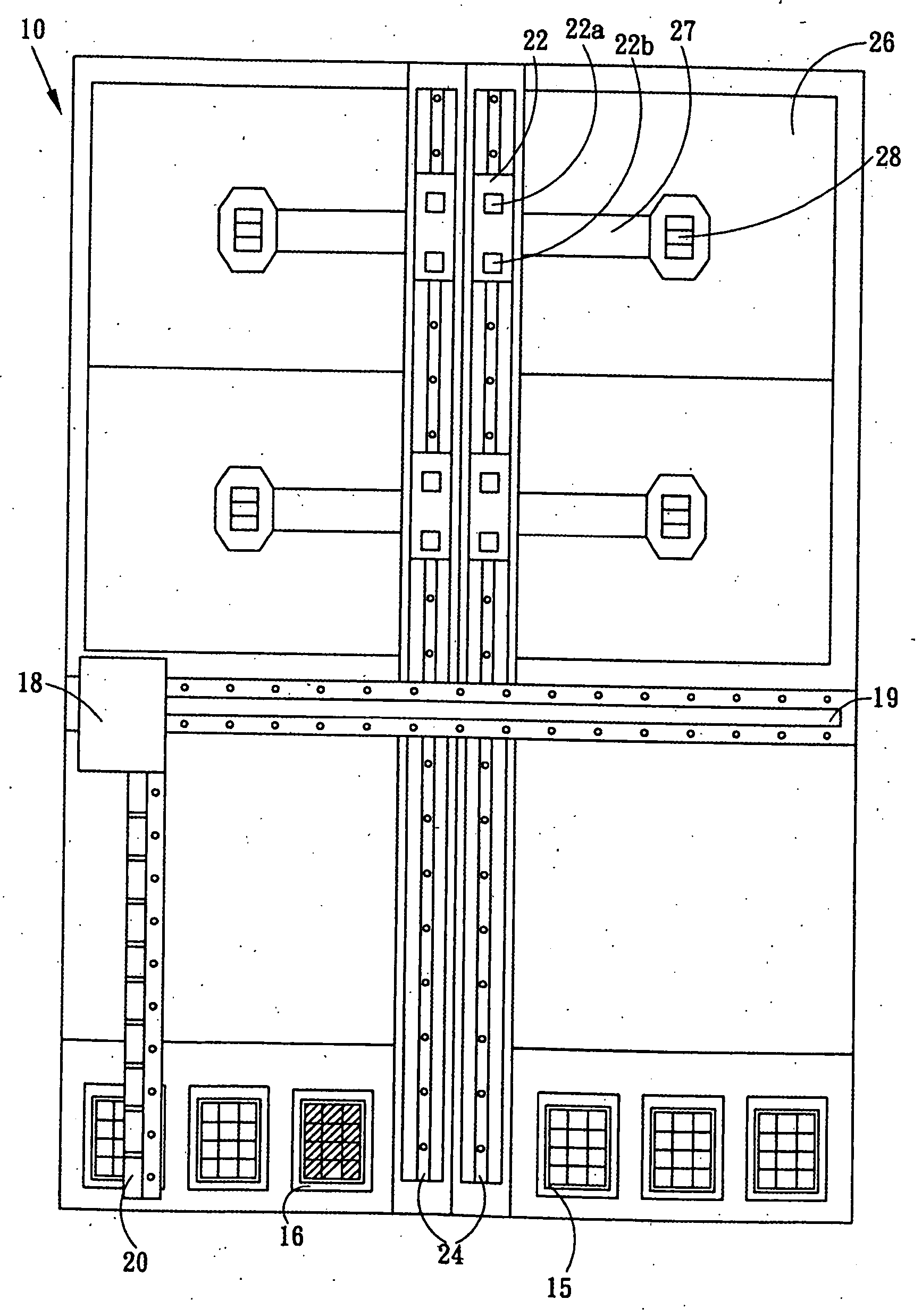
Figure 1 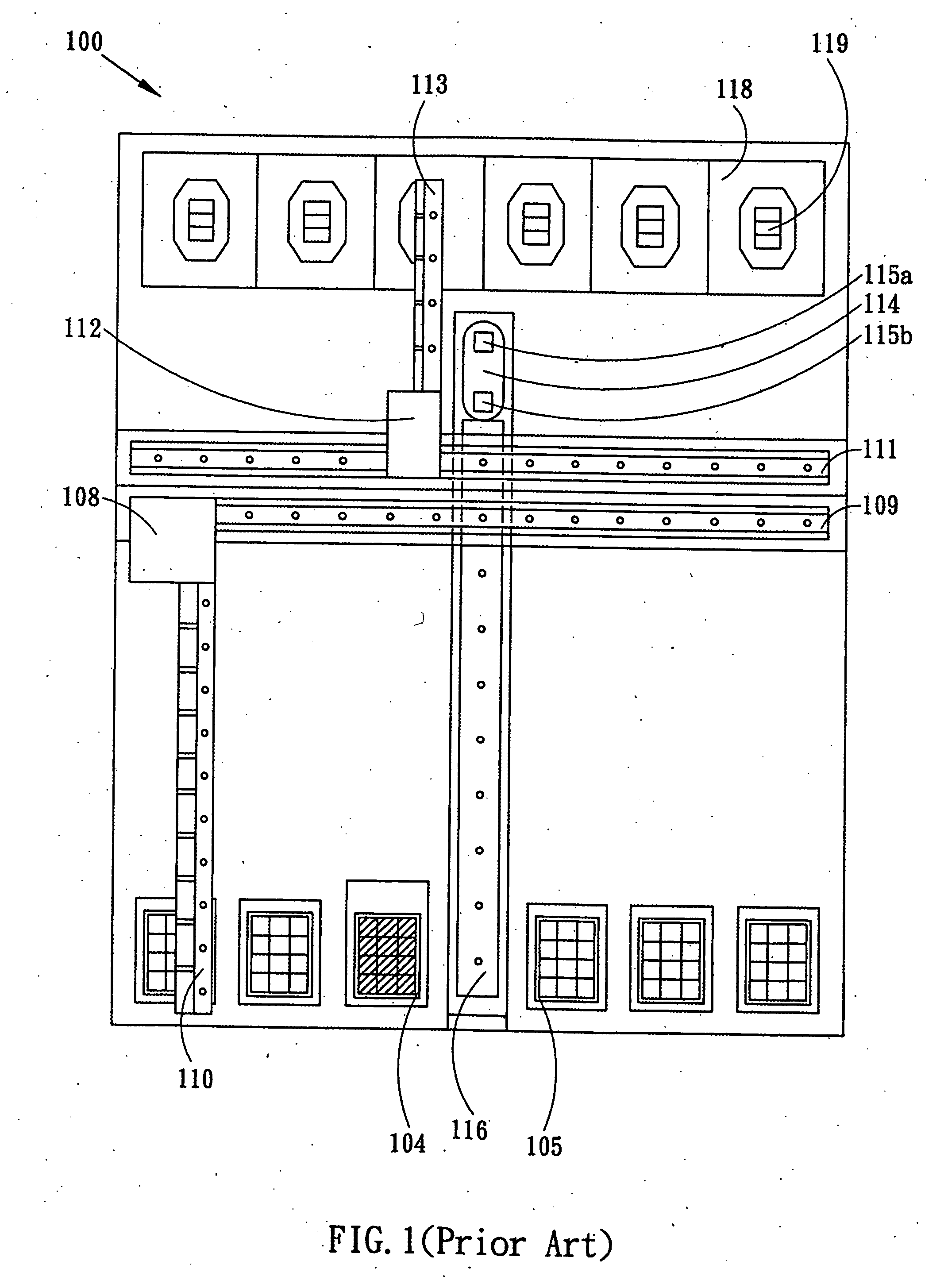
Figure 2 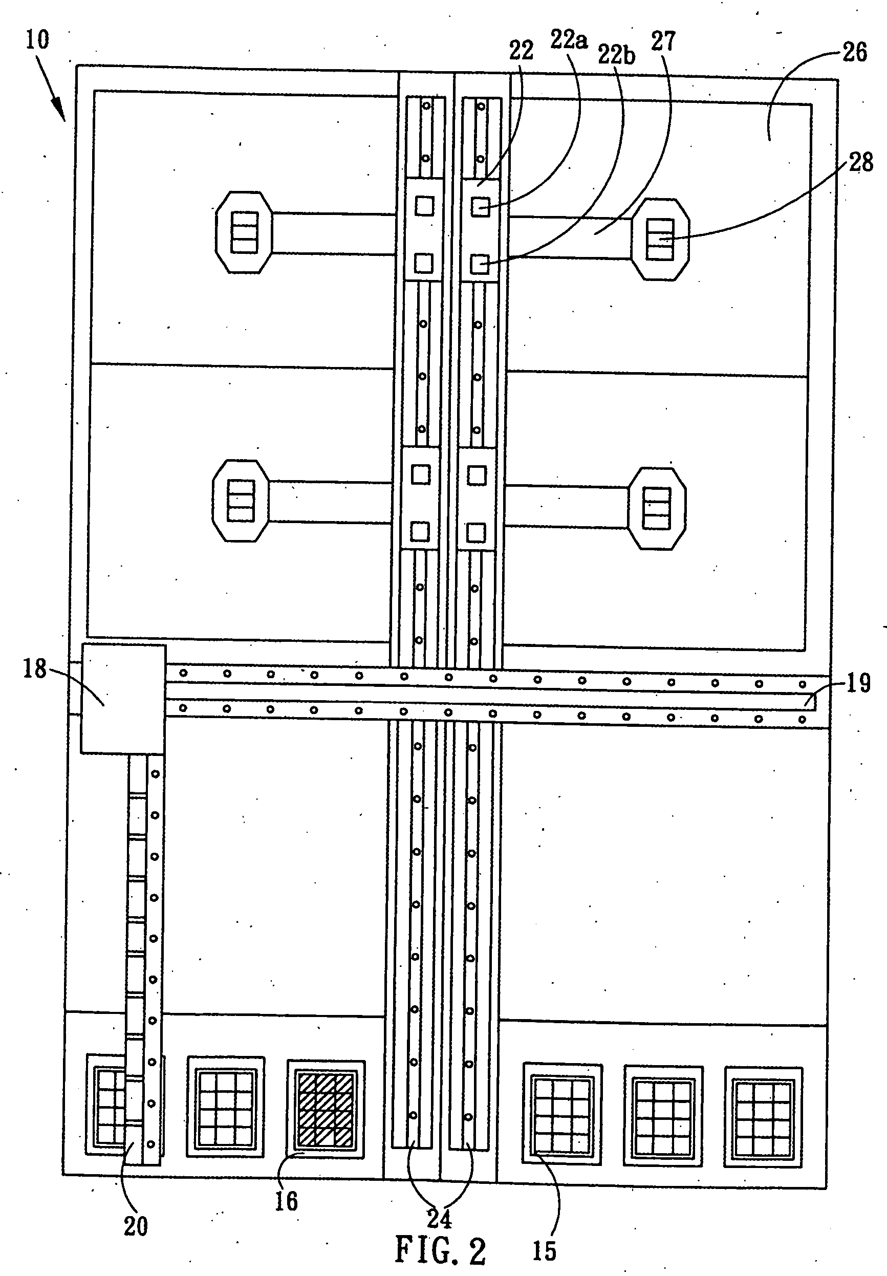
Figure 3
Abstract
Description
BACKGROUND OF THE INVENTION
[0001] 1. Field of the Invention
[0002] The present invention generally relates to an electronic component test device, and more particularly to an Integrated Circuit (ICs) test device, which includes a plurality of shuttles having individual pick and place module.
[0003] 2. Description of the Prior Art
[0004] During the packaging process, Integrated circuit (ICs) may be damaged or packaging may not be correctly performed. The failures introduced during packaging typically cause 1 percent or more of ICs to fail. Therefore it is necessary to perform the final test, which fully inspection performed on each packaged IC prior to shipment, in order to satisfy customer's requirement.
[0005] FIG. 1 shows the vertical plan view of conventional test apparatus (handler 100). The handler 100 is a piece of equipment that “handles” the ICs and makes connections to an automatic tester (not shown) via connecting cable. The handler can be divided into two zones, the input...
Examples
Embodiment Construction
[0018] The detailed description of the present invention will be discussed in the following embodiment, which is not intended to limit the scope of the present invention, but can be adapted for other applications. While drawings are illustrated in details, it is appreciated that the quantity of the disclosed components may be greater or less than that disclosed, except expressly restricting the amount of the components.
[0019]FIG. 2 shows the vertical plan view of ICs test apparatus according to one embodiment of the present invention. Pluralities of input trays 16 for storing the ICs are stacking arrangements in the input / output zone of the handler 10. Each of the input trays 16 with a plurality of IC aligned thereon. Similar to input trays 16, there is also at least one output tray 15 located within the input / output zone for storing the tested IC. The tested ICs are graded to output trays 15 according to measured parameter. The number of input / output trays 16 / 15 and their location...