

Sensing circuit for multi-level flash memory
a sensing circuit and flash memory technology, applied in the field of sensing circuits for multi-level flash memory, can solve the problems of limited storage capacity becoming a disadvantage, limited storage capacity being provided to generate the required number of reference voltage levels, and the limitation of one memory cell being able to distinguish only two different states, etc., to achieve the effect of reducing the global circuit dimension and reducing the testing time for reference voltage calibration
Patent Information
- Authority / Receiving Office
- US · United States
- Current Assignee / Owner
- Publication Date
- 2007-02-01
- Estimated Expiration
- Not applicable · inactive patent
Smart Images
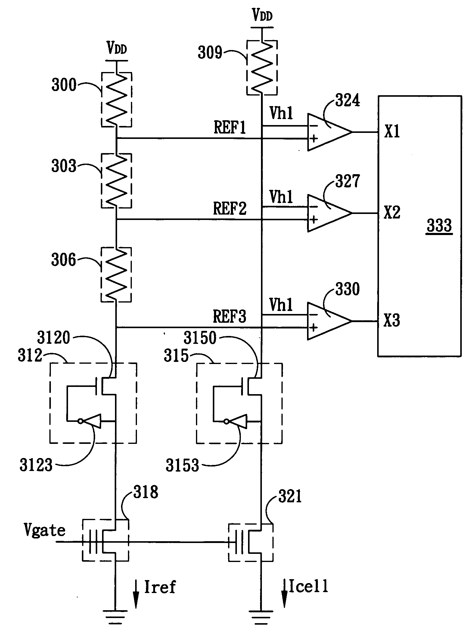
Figure 1 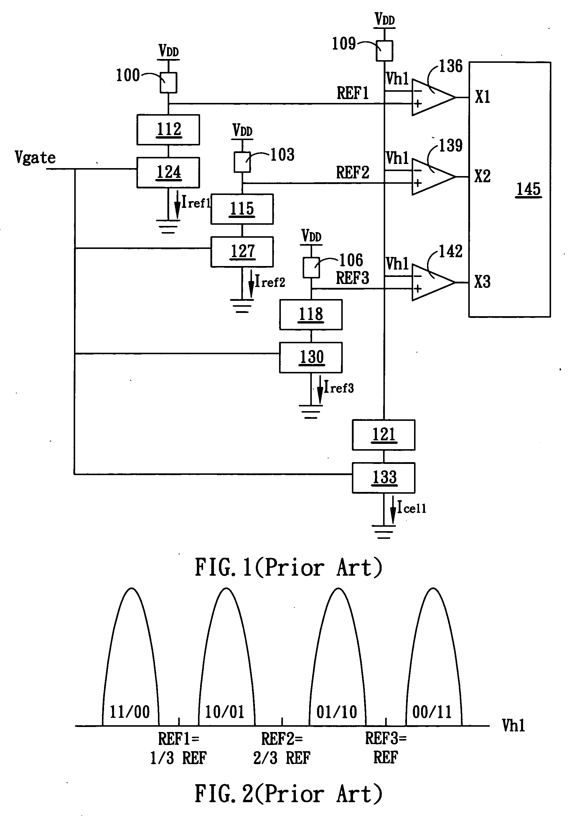
Figure 2 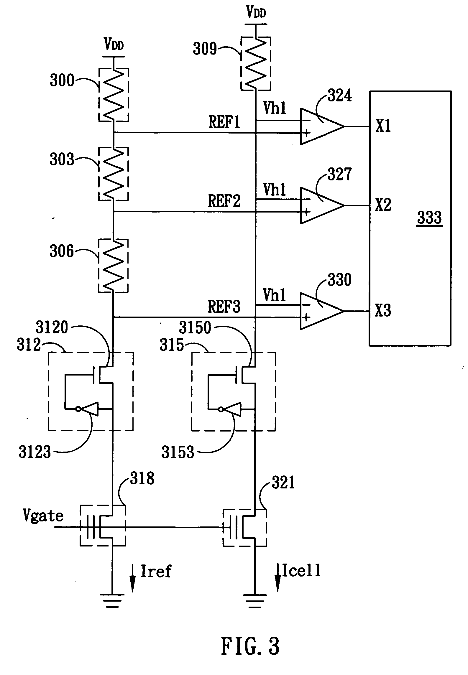
Figure 3
Abstract
Description
BACKGROUND OF THE INVENTION
[0001] 1. Field of the Invention
[0002] The present invention generally relates to a sensing circuit for multi-level flash memory, and more particularly to a sensing circuit for multi-level flash memory by using voltage division to provide reference voltages.
[0003] 2. Description of the Prior Art
[0004] In conventional memory devices, data is stored in a flash memory cell in the form of electrical charge accumulated inside an inner gate, which is known as a floating gate. The amount of charge stored in the floating gate depends on the voltage applied to the external gate of the memory cell that controls the magnitude of electrical current flowing through it. The data state “0”, or “1” represented by the memory cell depends on whether threshold voltage generated by the stored charge exceeds a specified threshold voltage or not. However, such conventional memory has the limitation that one memory cell can distinguish only two different states, i.e., one me...
Examples
Embodiment Construction
[0018] The detailed description of the present invention will be discussed in the following embodiment, which is not intended to limit the scope of the present invention, but can be adapted for other applications.
[0019] The present invention discloses a sensing circuit for multi-level flash memory capable of reducing global circuit dimension as well as decreasing the reference voltage calibration time. FIG. 3 shows the circuit diagram of one embodiment according to present invention. The diagram includes a reference voltage generator, a data saving circuit, a comparing circuit, and a decoder 333. The reference voltage generator contains a first resistive device 300, a second resistive device 303, a third resistive device 306, a first bit line clamp circuit 312, and a reference memory cell 318. Terminals of the first resistive device 300 are respectively connected to a voltage source VDD and the first terminal of the second resistive device 303. The second terminal of the second res...